Semiconductor device and manufacturing method thereof

A manufacturing method, semiconductor technology, applied in the direction of semiconductor/solid-state device manufacturing, semiconductor devices, electrical components, etc., can solve the problems that cannot meet the performance of MOSFET devices, can not completely eliminate short-channel effects and high leakage problems, and achieve improved short-circuit Channel effect, improvement of anti-short channel effect, effect of performance improvement

Pending Publication Date: 2019-07-23
SEMICON MFG INT (SHANGHAI) CORP +1
View PDF8 Cites 0 Cited by
  • Summary
  • Abstract
  • Description
  • Claims
  • Application Information

AI Technical Summary

Problems solved by technology

However, it is found in practice that these methods cannot completely eliminate the short channel effect and high leakage problems, and still cannot meet the requirements for further improvement of MOSFET device performance.

Method used


Image

  • Semiconductor device and manufacturing method thereof
  • Semiconductor device and manufacturing method thereof
  • Semiconductor device and manufacturing method thereof

Examples


Embodiment Construction

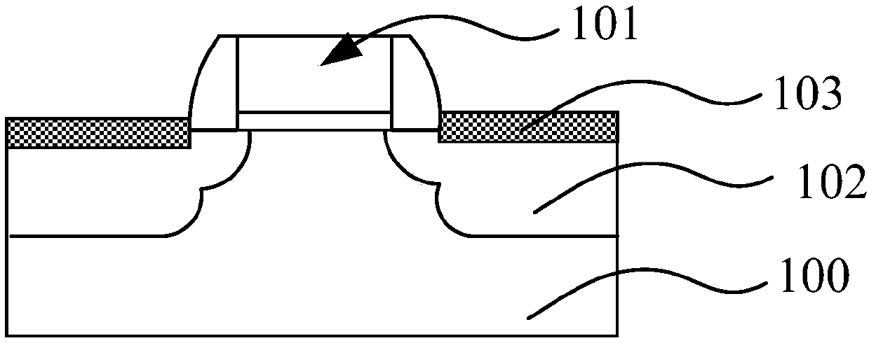
[0044] Please refer to figure 1 A MOS transistor includes a semiconductor substrate 100, a gate stack structure 101 formed on the surface of the semiconductor substrate 100, and LDD ion implantation regions 102 formed in the semiconductor substrate 100 on both sides of the gate stack structure 101 and The source and drain regions (i.e. source and drain regions) 103, the formation process of the source and drain regions 103 may include: etching the semiconductor substrate 100 on both sides of the gate stack structure 101 to form source and drain grooves; The growth process directly epitaxially grows a source-drain stress layer (silicon germanium for PMOS transistors and silicon carbon for NMOS transistors) in the source-drain grooves, thereby forming embedded source / drain regions 103 .

[0045]As mentioned in the background art, as the gate length of transistors shrinks, for example, after entering the 28nm technology node, the short channel effect (SCE) and the reverse short c...


PUM

PropertyMeasurementUnit
Thicknessaaaaaaaaaa

Abstract

The invention provides a semiconductor device and a manufacturing method thereof. A diffusion barrier layer is formed on the side wall of a source and drain groove, on one hand, the stress, introducedtowards a channel region, of a stress layer of epitaxial growth in the source and drain groove subsequently cannot be reduced, on the other hand, subsequently formed doped ions in the stress layer further can be avoided from being diffused into the channel region and a gate medium layer, the junction depth is avoided form being increased, and the redistribution of the doped ions is avoided, so that the short-channel effect and reverse short-channel effect are improved, and the requirement that the performance of the device is improved is met.

Description

technical field [0001] The invention relates to the technical field of integrated circuit manufacturing, in particular to a semiconductor device and a manufacturing method thereof. Background technique [0002] After MOSFET devices are scaled down to 45nm and below, short channel effect (SCE) and reverse short channel effect (RSCE) become the key constraints to improve the performance of MOSFET devices as the gate length of transistors shrinks. At present, the industry usually performs lightly doped drain (lightly dopeddrain, LDD) ion implantation in the semiconductor substrate on both sides of the gate stack structure to form an ultra shallow junction, so as to improve the SCE effect and RSCE effect, and through amorphization ion implantation (pre-amorphization implant, PAI) and introducing stress into the channel to further optimize the distribution of ions implanted in LDD, etc., to improve device performance. However, it is found in practice that these methods cannot co...

Claims


Application Information

Patent Timeline
IPC IPC(8): H01L21/336H01L21/28H01L29/08H01L29/423H01L29/78
CPCH01L29/66636H01L29/7848H01L29/42356H01L29/0847
Inventor 赵猛
Owner SEMICON MFG INT (SHANGHAI) CORP
Why Eureka
Try Eureka