

Semiconductor laser device non-absorption window and preparation method thereof, and semiconductor laser device
A laser and non-absorbing technology, applied in the direction of semiconductor lasers, lasers, laser components, etc., can solve the problems of reducing device reliability, increasing production costs, and long diffusion time, so as to reduce reliability, increase costs, and long diffusion time Effect
- Summary
- Abstract
- Description
- Claims
- Application Information
AI Technical Summary
Problems solved by technology
Method used
Image

Examples
Embodiment Construction
[0023] In order to make the purpose, technical solutions and advantages of the embodiments of the present invention clearer, the technical solutions in the embodiments of the present invention will be clearly and completely described below in conjunction with the drawings in the embodiments of the present invention. Obviously, the described embodiments It is a part of embodiments of the present invention, but not all embodiments. Based on the embodiments of the present invention, all other embodiments obtained by those skilled in the art without making creative efforts belong to the protection scope of the present invention.
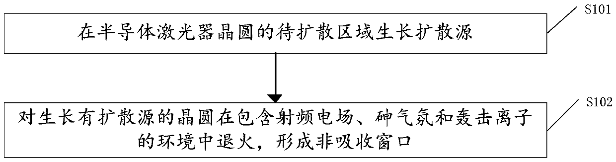
[0024] An embodiment of the present invention provides a method for fabricating a non-absorbing window of a semiconductor laser, such as figure 1 As shown, the preparation method includes the following steps:
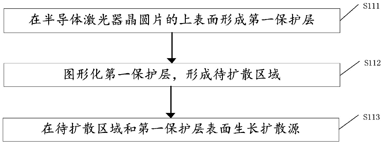
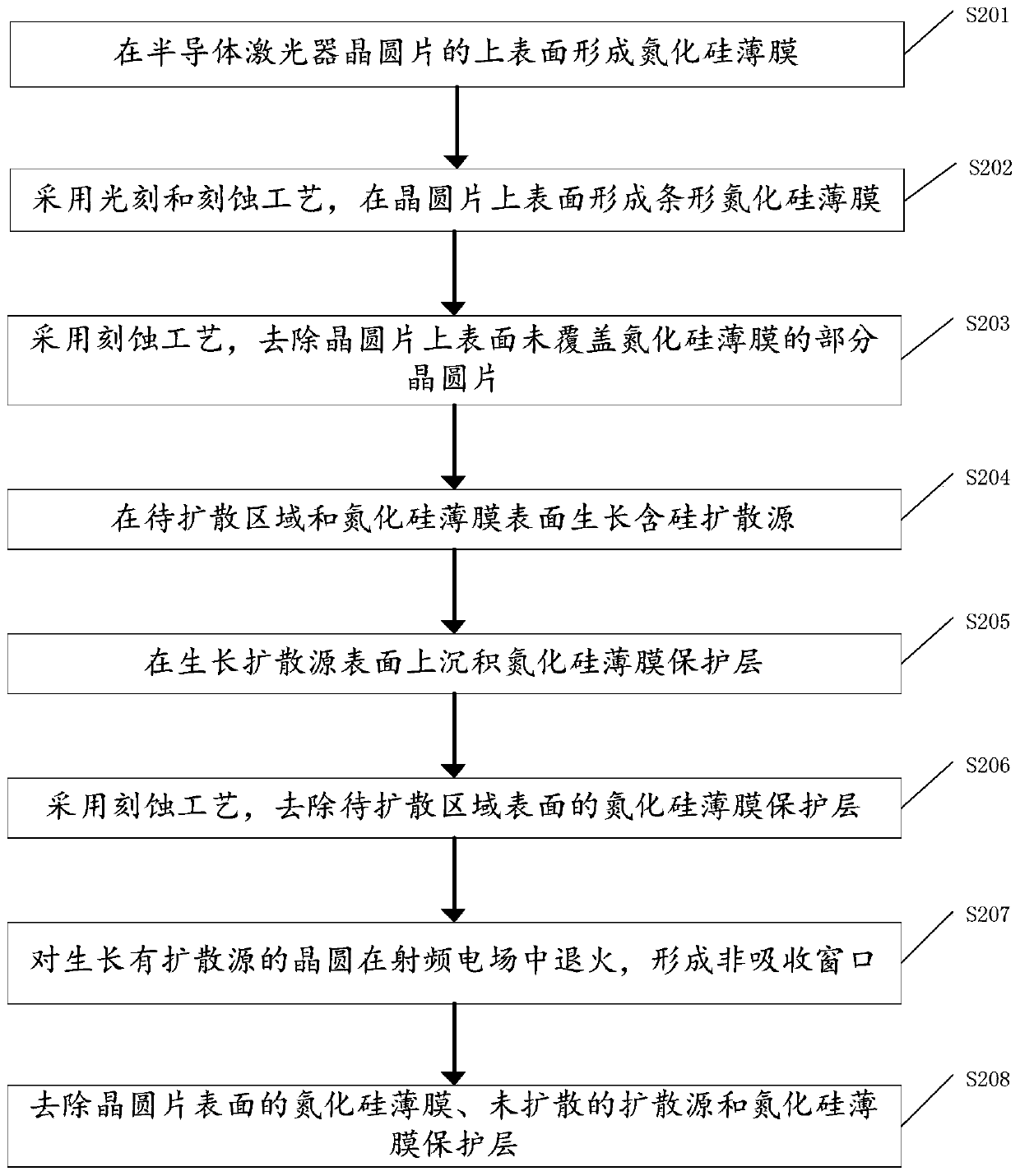
[0025] S101: growing a diffusion source in a region to be diffused on a semiconductor laser wafer. Specifically, the structure of a semiconduct...
PUM
 Abstract
Description
Claims
Application Information