Method for processing thermoelectric separation substrate for LED

A processing method and technology of thermoelectric separation, applied in circuits, electrical components, semiconductor devices, etc., can solve the problems of thermoelectric separation substrates failing to dissipate heat, difficult to control the amount of glue overflowing, affecting heat conduction, etc., to achieve tight integration and improved production efficiency. , the effect of good insulation performance

Active Publication Date: 2019-08-09
AKM ELECTRONICS INDAL PANYU
View PDF7 Cites 4 Cited by
  • Summary
  • Abstract
  • Description
  • Claims
  • Application Information

AI Technical Summary

Problems solved by technology

[0005] In the prior art, the thermoelectric separation substrate is laminated at high temperature, and the substrate, PP and copper foil are laminated and pressed together. However, during the lamination process, it is difficult to control the amount of glue overflow, and the resin glue in PP will overflow into the hot channel. On the pad, the resin glue remaining on the thermal channel pad will affect the heat conduction, so that the heat dissipation effect of the thermoelectric separation substrate cannot be guaranteed

Method used


Image

  • Method for processing thermoelectric separation substrate for LED
  • Method for processing thermoelectric separation substrate for LED

Examples


Embodiment Construction

[0020] The following will clearly and completely describe the technical solutions in the embodiments of the present invention with reference to the drawings in the embodiments of the present invention.

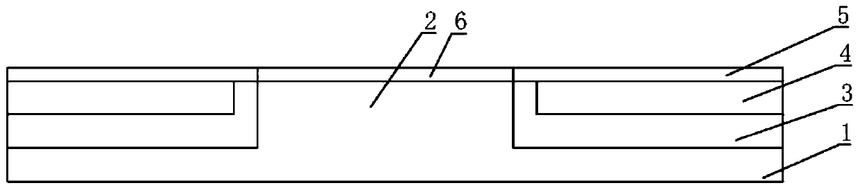
[0021] See figure 1 The thermoelectric separation substrate produced by the processing method of the thermoelectric separation substrate for LED of the present invention includes a copper substrate 1, a boss 2 on the copper substrate, a PP sheet 3 on both sides of the boss 2, and copper on the PP sheet 3. Foil 4, copper foil 4 is coated with ink 5 for solder resist, boss 2 is subjected to OSP surface treatment, and a layer of organic solder protection film 6 is grown chemically on the clean bare copper surface of boss 2 .

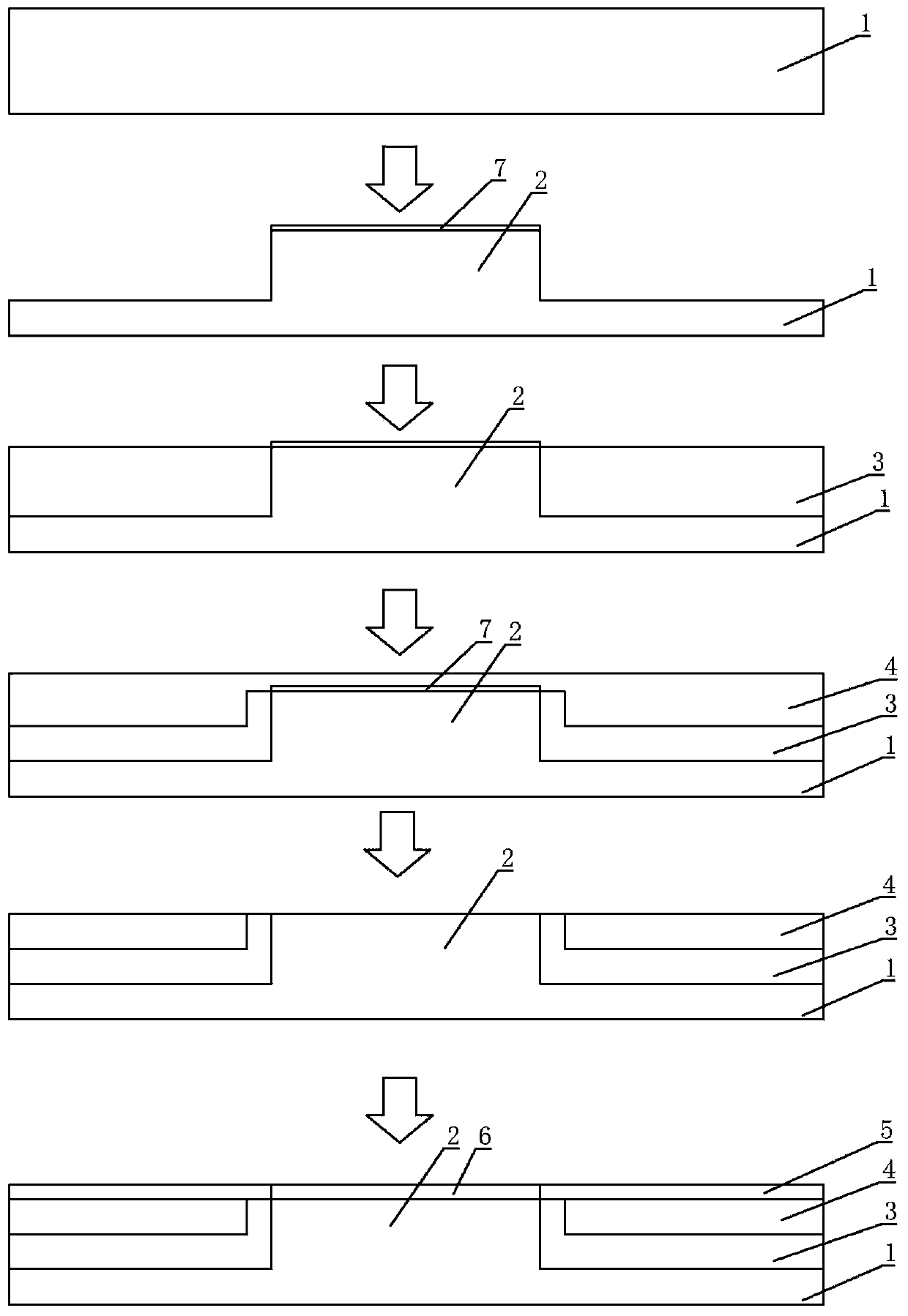
[0022] The above-mentioned processing method for a thermoelectric separation substrate for LEDs comprises the following steps: cutting the copper substrate, drilling an alignment tool hole on the copper substrate, then covering the copper substrate with a ...


PUM


Abstract

The invention provides a method for processing a thermoelectric separation substrate for an LED. The method can prevent the overflowed glue generated in the manufacturing process of the thermoelectricseparation substrate from affecting the heat dissipation effect of the thermoelectric separation substrate, and includes the following steps of: cutting a copper substrate; drilling an alignment toolhole on the copper substrate, covering the copper substrate with a dry film, performing exposure and development, performing depth-controlling etching on the exposed and developed copper substrate, forming, on the copper substrate, a boss in contact with and thermally conductive with the LED; browning the copper substrate, attaching a PP sheet to the copper substrate, windowing the PP sheet at aposition corresponding to the boss; covering the PP sheet with a layer of copper foil, wherein the copper foil, the PP sheet, the copper substrate are laminated from top to bottom; performing a dry film pretreatment on the copper foil, attaching the dry film, performing exposure and development, removing the copper foil on the dry film of the boss by etching and windowing, manufacturing a circuit,and then removing the dry film on the boss to expose the boss.

Description

technical field [0001] The invention relates to the technical field of circuit board production, in particular to a method for processing a thermoelectric separation substrate for LEDs. Background technique [0002] As a new generation of solid-state light source, light-emitting diode (Light-Emitting Diode, referred to as LED) has many advantages such as long life, high efficiency, energy saving, green environmental protection, etc., and is widely used in lighting sources. It is widely used in semiconductor production, so that the luminous efficiency of LED can be continuously improved and the cost can be continuously reduced. [0003] The core part of the LED is the PN junction. When the injected electrons and holes recombine at the PN junction, the electrical energy is directly converted into light energy, but not all the converted light energy can be emitted out of the LED, it will be in the PN junction and epoxy The resin / silica gel is converted into heat energy by the ...

Claims


Application Information

Patent Timeline
Patent Type & Authority Applications(China)
IPC IPC(8): H01L33/62H01L33/64H01L33/48
CPCH01L33/483H01L33/62H01L33/647H01L2933/0033H01L2933/0066H01L2933/0075
Inventor 赵苗枫潘丽董异文
Owner AKM ELECTRONICS INDAL PANYU
Why Eureka
Try Eureka