A kind of nitride led manufacturing method based on metal mask substrate

A metal mask and manufacturing method technology, applied in semiconductor devices, electrical components, circuits, etc., can solve problems such as increasing device leakage current, device damage, affecting device light extraction efficiency, performance and stability, and improving heat dissipation. performance, improved crystal quality, strong absorption effect

Active Publication Date: 2021-05-25
XIAMEN UNIV
View PDF7 Cites 0 Cited by
  • Summary
  • Abstract
  • Description
  • Claims
  • Application Information

AI Technical Summary

Problems solved by technology

Because GaN is decomposed into metal Ga and nitrogen gas at high temperature (900-1000°C) during this process, and a shock wave is generated, which will cause damage to the device after laser lift-off, increase the leakage current of the device, and affect the light extraction efficiency and performance of the device. and stability

Method used


Image

  • A kind of nitride led manufacturing method based on metal mask substrate
  • A kind of nitride led manufacturing method based on metal mask substrate
  • A kind of nitride led manufacturing method based on metal mask substrate

Examples


Embodiment 1

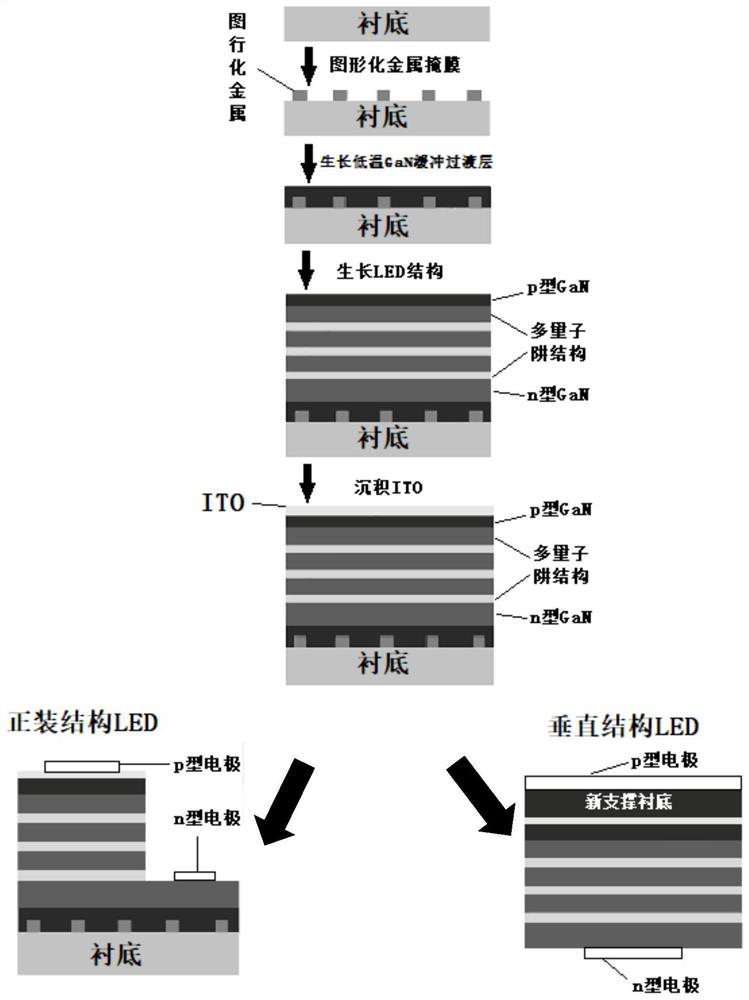
[0049] Embodiment 1: The preparation of front-mounted c-plane LED, see figure 2 .

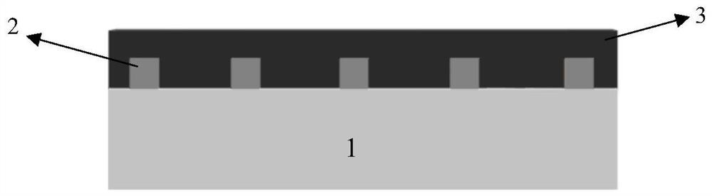
[0050] 1. The substrate can be sapphire, silicon carbide, Si and other substrates. Using photolithography technology, a patterned photoresist with an opening size of 1-500 μm and a duty ratio (without photoresist: with photoresist) of 1: (10-1) is formed on the substrate. The pattern can be: Long rectangles, regular hexagons or circles, etc., the single-layer patterns can be arranged in an equiperiod arrangement or a disordered arrangement; then magnetron sputtering technology is used to deposit a metal with a melting point greater than 1000°C on the substrate, with a thickness of In 10 ~ 150nm. The patterned metal layer can be a single layer or multiple layers, and the pattern direction and deposition thickness of each layer can be designed according to needs. After the metal deposition is completed, the photoresist is removed by using acetone or other solutions that can remove the photore...

Embodiment 2

[0060] Example 2: Preparation of c-plane vertical structure LED:

[0061]1. The substrate can be sapphire, silicon carbide, Si and other substrates. Using photolithography technology, a patterned photoresist with an opening size of 1-500 μm and a duty ratio (without photoresist: with photoresist) of 1: (10-1) is formed on the substrate. The pattern can be: Long rectangles, regular hexagons or circles, etc., the single-layer patterns can be arranged in an equiperiod arrangement or a disordered arrangement; then magnetron sputtering technology is used to deposit a metal with a melting point greater than 1000°C on the substrate, with a thickness of In 10 ~ 150nm. The patterned metal layer can be a single layer or multiple layers, and the pattern direction and deposition thickness of each layer can be designed according to needs. After the metal deposition is completed, the photoresist is removed by using acetone or other solutions that can remove the photoresist without damagin...

Embodiment 3

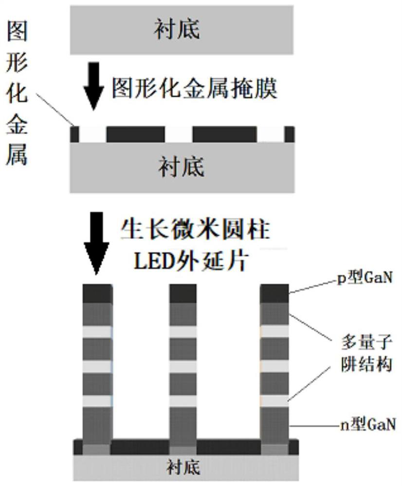
[0075] Embodiment 3: Preparation of micro-cylindrical LED epitaxial wafer:

[0076] 1. The substrate can be sapphire, silicon carbide, Si and other substrates. Using photolithography technology, a patterned photoresist with an opening size of 100nm to 10μm and a duty ratio (with photoresist: without photoresist) of 1: (10~1) is formed on the substrate. The pattern can be: Long rectangles, regular hexagons or circles, etc., the single-layer patterns can be arranged in an equiperiod arrangement or a disordered arrangement; then magnetron sputtering technology is used to deposit a metal with a melting point greater than 1000°C on the substrate, with a thickness of In the range of 10-150nm, the pattern direction and deposition thickness of each layer can be designed according to needs. After the metal deposition is completed, the photoresist is removed by using acetone or other solutions that can remove the photoresist without damaging the epitaxial wafer, and ultrasonic cleaning...


PUM

PropertyMeasurementUnit
thicknessaaaaaaaaaa
thicknessaaaaaaaaaa
melting pointaaaaaaaaaa

Abstract

The invention relates to a method for manufacturing a nitride LED based on a metal mask substrate, which relates to a semiconductor light emitting diode device. Form a transition layer on the substrate; use a single epitaxial growth technology or a combination of various epitaxial growth technologies to grow LED epitaxial wafers on the transition layer; use deposition technology to deposit ITO with a thickness of 10-200nm on the above-mentioned LED epitaxial wafers, and perform annealing ; For the LED epitaxial wafer deposited with ITO, perform photolithography, etching, electrode growth and packaging processes to prepare the formal LED; or after transferring the substrate, use separation techniques such as laser lift-off to separate the epitaxial wafer from the original substrate , and then carry out processes such as photolithography, etching, electrode growth and packaging, that is, to prepare vertical structure LEDs. The heat dissipation performance of the LED can be effectively improved, and the reliability of the LED device can be improved. Metal has good thermal conductivity, thereby realizing high-reliability LED operation and prolonging the life of LED.

Description

technical field [0001] The invention relates to a semiconductor light emitting diode (LED) device, in particular to a method for manufacturing a nitride LED based on a metal mask substrate. Background technique [0002] Nitride semiconductor is a kind of wide bandgap direct bandgap semiconductor, and its luminescence covers the entire visible light range. It has broad application prospects in semiconductor lighting, micro-display and other aspects. [0003] At present, the vast majority of commercial nitride LED devices use sapphire substrates. Because the thermal conductivity of sapphire substrates is poor, the efficiency of high-power light-emitting devices cannot be significantly improved. Therefore, in order to improve the heat dissipation performance of high-power LEDs, To solve problems such as the efficiency of traditional planar devices, vertical structures have been proposed. This technical route mainly uses laser lift-off, electroplating or bonding processes to t...

Claims


Application Information

Patent Timeline
Patent Type & Authority Patents(China)
IPC IPC(8): H01L33/22H01L33/32H01L33/00
CPCH01L33/0075H01L33/22H01L33/32H01L33/0093
Inventor 龙浩冯笑杰田梦飞张保平应磊莹
Owner XIAMEN UNIV
Why Eureka
Try Eureka