Nonpolar self-supporting Gan-based pin ultraviolet photodetector and preparation method

An electrical detector, self-supporting technology, applied in circuits, electrical components, semiconductor devices, etc., can solve the problems of large polarized electric field, uneven internal electric field, difficult p-type doping, etc.

Active Publication Date: 2021-02-02
JIANGSU INST OF ADVANCED SEMICON CO LTD
View PDF10 Cites 0 Cited by
  • Summary
  • Abstract
  • Description
  • Claims
  • Application Information

AI Technical Summary

Problems solved by technology

[0005] In order to solve the deficiencies in the prior art, the object of the present invention is to provide a pin ultraviolet photodetector based on a non-polar self-supporting GaN substrate and its preparation method, to solve the problem of large polarization electric field and Lattice mismatch between the epitaxial layer and the substrate, difficult p-type doping, and uneven internal electric field, and simplify the fabrication process of the ultraviolet photodetector chip

Method used


Image

  • Nonpolar self-supporting Gan-based pin ultraviolet photodetector and preparation method

Examples


Embodiment Construction

[0028] The implementation of the present invention will be further described below in conjunction with the accompanying drawings and examples, but the implementation and protection of the present invention are not limited thereto.

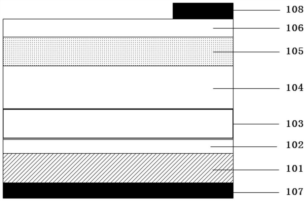
[0029] The invention provides a nonpolar self-supporting GaN-based pin ultraviolet photodetector. refer to figure 1 , the detector includes a non-polar self-supporting GaN substrate 101, an n-type GaN layer 102, an n-type Al x1 Ga 1-x1 N graded layer 103, intrinsic Al 0.4 Ga 0.6 N layer 104, p-type Al 0.45 Ga 0.55 N / Al 0.4 Ga 0.6 N superlattice layer 105 , p-type GaN capping layer 106 , n-type ohmic electrode 107 and p-type ohmic electrode 108 . Among them, the nonpolar self-supporting GaN substrate 101 has a thickness of 300 μm; the n-type GaN layer 102 is located on the front surface of the nonpolar self-supporting GaN substrate 101, its thickness is 100 nm, and the doping concentration is 5×10 18 cm -3 ; n-type Al x1 Ga 1-x1 The N grad...


PUM

PropertyMeasurementUnit
thicknessaaaaaaaaaa
thicknessaaaaaaaaaa
thicknessaaaaaaaaaa

Abstract

The invention discloses a nonpolar self-supporting GaN-based pin ultraviolet photodetector and a preparation method thereof. The detector comprises a nonpolar self-supporting GaN substrate, an n-type GaN layer, an n-type Al x1 Ga 1‑x1 N graded layer, intrinsic Al x2 Ga 1‑x2 N layer, p-type Al y1 Ga 1‑y1 N / Al y2 Ga 1‑y2 The N superlattice layer and the p-type GaN capping layer are arranged sequentially from bottom to top; the back of the non-polar self-supporting GaN substrate is connected to the n-type ohmic electrode; the upper surface of the p-type GaN capping layer is connected to the p-type ohmic electrode . The detector solves the problems of large polarization electric field, lattice mismatch between the epitaxial layer and the substrate, difficult p-type doping, and uneven internal electric field, and simplifies the preparation process of the ultraviolet photodetector chip.

Description

technical field [0001] The invention relates to the technical field of semiconductor devices, in particular to a nonpolar self-supporting GaN-based pin ultraviolet photodetector and a preparation method. Background technique [0002] Ultraviolet detection technology is a new type of photoelectric detection technology, which is widely used in national defense and military fields such as precision guidance and ultraviolet high-security communication. It has applications in environmental pollution monitoring, biological analysis, astronomy, and flame detection in civilian applications. Gallium nitride (GaN) and its series of materials, as the third-generation semiconductors, have the advantages of large band gap and wide spectral range, and have great application value in the field of optoelectronics. GaN-based ternary alloy AlGaN is a direct bandgap semiconductor. The bandgap can change continuously with the Al composition from 3.4eV to 6.2eV. The peak response wavelength rang...

Claims


Application Information

Patent Timeline
Patent Type & Authority Patents(China)
IPC IPC(8): H01L31/0224H01L31/024H01L31/0304H01L31/0352H01L31/105H01L31/18
CPCH01L31/022408H01L31/024H01L31/03042H01L31/03048H01L31/035236H01L31/035272H01L31/03529H01L31/105H01L31/1848Y02P70/50
Inventor 尹以安李锴曾妮
Owner JIANGSU INST OF ADVANCED SEMICON CO LTD
Why Eureka
Try Eureka