Nitride multi-junction solar cell and preparation method thereof

A solar cell and nitride technology, applied in the field of solar cells, can solve the problem of absorbing a large number of ultraviolet photons, and achieve the effect of improving light conversion rate and promoting absorption

Pending Publication Date: 2019-08-16
SHENZHEN KECHUANG DIGITAL DISPLAY TECH
View PDF0 Cites 1 Cited by
  • Summary
  • Abstract
  • Description
  • Claims
  • Application Information

AI Technical Summary

Problems solved by technology

The setting of the quantum dot material layer can effectively solve the problem that the current diffusion layer on the surface of the InGaN top cell will absorb a large amount of ultraviolet photons, and can effectively improve the external quantum efficiency in the ultraviolet band

Method used


Image

  • Nitride multi-junction solar cell and preparation method thereof
  • Nitride multi-junction solar cell and preparation method thereof

Examples


Embodiment 1

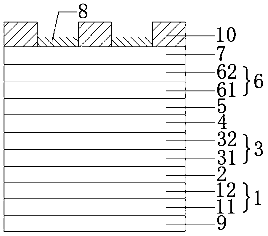
[0027] see figure 1 , the present embodiment provides a nitride multi-junction solar cell, comprising an InN bottom cell 1, an AlN nucleation layer one 2, a Si sub-cell 3, an AlN nucleation layer two 4, a GaN buffer layer 5, and an InGaN top cell arranged in sequence 6. The current diffusion layer 7 and the quantum dot material layer 8 arranged on the current diffusion layer, the InN bottom cell 1 includes an n-type InN layer 11 and a p-type InN layer 12, and the Si sub-cell 3 includes an n-type Si layer 31 and p-type Si layer 32. The InGaN top cell 6 includes an n-type InGaN layer 61 and a p-type InGaN layer 62. In this implementation, the n-type InGaN layer 61 is n-type In 0.33 Ga 0.67 N layer, p-type InGaN layer 62 is p-type In 0.33 Ga 0.67 N layer, in the present embodiment, the current diffusion layer 7 is an ITO layer, and the material used in the quantum dot material layer 8 is CdS quantum dots, and a negative electrode 91 is arranged at the bottom of the InN bottom ...

Embodiment 2

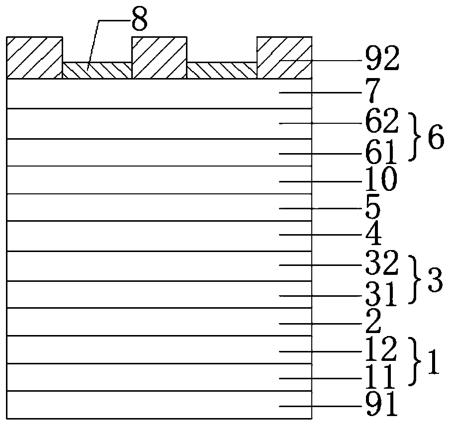
[0040] see figure 2 , the present embodiment provides a nitride multi-junction solar cell, comprising an InN bottom cell 1, an AlN nucleation layer 1, a Si sub-cell 3, an AlN nucleation layer 2 4, a GaN buffer layer 5, and a BInGaN layer 10 arranged in sequence , an InGaN top cell 6, a current diffusion layer 7 and a quantum dot material layer 8 disposed on the current diffusion layer, the InN bottom cell 1 includes an n-type InN layer 11 and a p-type InN layer 12, and the Si sub-cell 3 includes an n-type Si layer 31 and a p-type Si layer 32, and the InGaN top cell 6 includes an n-type InGaN layer 61 and a p-type InGaN layer 62. In this embodiment, the n-type InGaN layer 61 is n-type In 0.33 Ga 0.67 N layer, p-type InGaN layer 62 is p-type In 0.33 Ga 0.67 N layer, in the present embodiment, the current diffusion layer 7 is an ITO layer, and the material used in the quantum dot material layer 8 is CdS quantum dots, and a negative electrode 9 is arranged at the bottom of the...

Embodiment 3

[0044] This embodiment provides a nitride multi-junction solar cell In 0.28 Ga 0.72 N / Si / InN, the preparation steps are the same as in Example 2, except that the InGaN top cell grown in step (3) includes n-type In 0.28 Ga 0.72 N-layer and n-type In 0.28 Ga 0.72 N layers.


PUM

PropertyMeasurementUnit
thicknessaaaaaaaaaa

Abstract

The invention discloses a nitride multi-junction solar cell and a preparation method thereof. The nitride multi-junction solar cell comprises an InN bottom cell, an AlN nucleation layer I, a Si sub-cell, an AlN nucleation layer II, a GaN buffer layer, an InGaN top cell, a current diffusion layer and a quantum dot material layer on the current diffusion layer, which are arranged in sequence. The nitride multi-junction solar cell provided by the invention can promote the absorption of photons of larger wavelength and improve the light conversion rate, and the quantum dot material layer can improve the external quantum efficiency of the ultraviolet band.

Description

technical field [0001] The invention relates to the technical field of solar cells, in particular to a nitride multi-junction solar cell and a preparation method thereof. Background technique [0002] Nitride semiconductor materials are adjustable in a wide range of electron motion, so the energy band width range is large, and the band gap is significantly larger than that of Si and other semiconductor materials. It has important applications in many fields such as transistors, new solar cells, and semiconductor lighting. [0003] In a solar cell, since the incident photons will be absorbed by the material successively according to the order of energy level. That is, light with short wavelengths will be absorbed first, while light with long wavelengths will be absorbed last due to the deeper penetration depth of photons. The energy of a photon must be greater than the energy gap Eg (Energy gap) of the material. In other words, the wavelength of the incident light entering t...

Claims


Application Information

Patent Timeline
Patent Type & Authority Applications(China)
IPC IPC(8): H01L31/0687H01L31/18
CPCH01L31/0687H01L31/18Y02E10/544Y02P70/50
Inventor 郭建廷李方红常嘉兴
Owner SHENZHEN KECHUANG DIGITAL DISPLAY TECH
Why Eureka
Try Eureka