Read-out circuit and working method thereof

A readout circuit and circuit technology, applied in the field of readout circuits, can solve the problems of increasing circuit area and cost, test structure interference, and high device requirements, and achieve the effects of complete coverage, shortened test time, and accurate test results.

Active Publication Date: 2019-08-20
北京安酷智芯科技有限公司
View PDF5 Cites 8 Cited by
  • Summary
  • Abstract
  • Description
  • Claims
  • Application Information

AI Technical Summary

Problems solved by technology

However, the test of the uncooled infrared detector readout circuit still faces the following two problems: how to achieve a comprehensive test without MEMS sensors and how to complete the function / performance test of each part of the column channel readout circuit
Since a large number of MEMS sensors are required on the entire sensor array, replacing them all with polysilicon resistors of equal resistance will greatly increase the area and cost of the circuit, and setting alternative resistors or current and voltage outside the array for testing cannot fully simulate the growth of MEMS sensors. The working environment of the chip, such as the influence of parasitic capacitance and resistance, will greatly reduce the validity of the test results obtained; moreover, since the CMOS readout circuit usually adopts the column-level readout method, the layout of each column readout circuit is more than ten microns The vertical strips are wide and hundreds of microns high, and the step-by-step modules of the readout channel, such as front-end differential amplifiers, integrators, and analog-to-digital converters, are placed in sequence
If the readout circuit module is placed separately outside the array, there will be a problem that the parasitic environment is inconsistent with the actual array, and the complexity of the design will be increased; while testing in the array may cause the original readout circuit to be tested Structural interference; and when there is a MEMS sensor in the readout circuit, the traditional method is to change the bias voltage, and then reverse the resistance value of the resistor according to the estimated current change to the output gain, but this method is effective The premise is that the gain uniformity of the column level is good and the process angle error of the capacitance and resistance of the readout circuit is small, which is extremely demanding on the device

Method used


Image

  • Read-out circuit and working method thereof
  • Read-out circuit and working method thereof
  • Read-out circuit and working method thereof

Examples


Embodiment 1

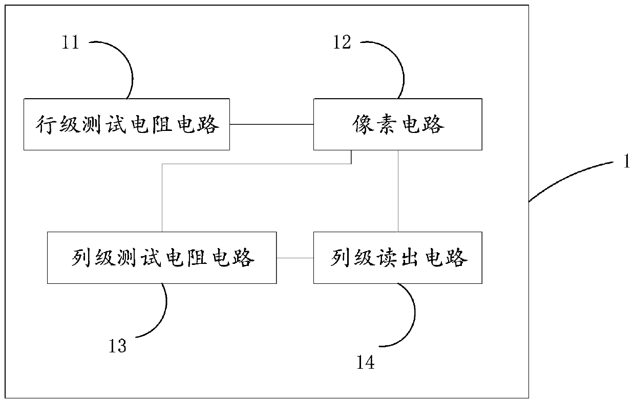
[0039] like figure 1 As shown, the present embodiment discloses a readout circuit 1, and the readout circuit includes: M columns×N rows of pixel circuits 12, N rows of row-level test resistor circuits 11, M columns of column-level test resistor circuits 13, and M columns Column-level readout circuit 14; wherein M and N are natural numbers and M≥2, N≥2;

[0040] The row-level test resistor circuit 11, the column-level test resistor circuit 13, and the column-level readout circuit 14 are all connected to the pixel circuit 12; the column-level test resistor circuit 13 is connected to the column-level readout circuit 12; The circuit 14 is connected; wherein, the column-level readout circuit 14 includes a test column sub-circuit; the column-level readout circuit 14 is also connected with a current source.

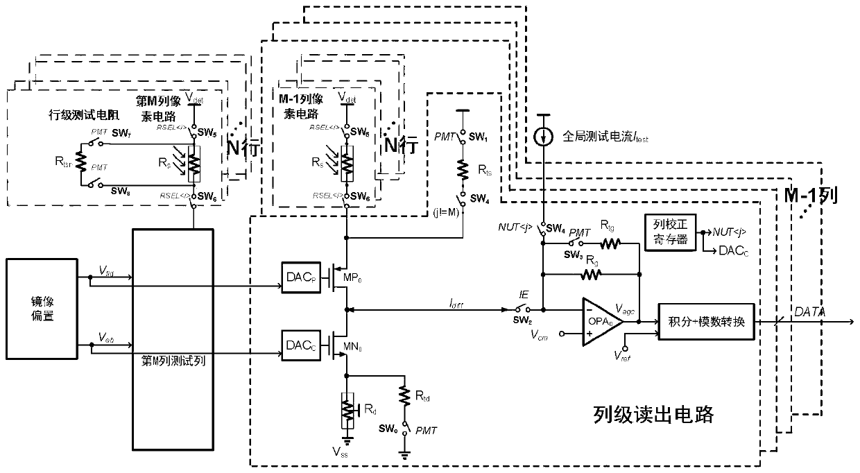
[0041] like figure 2 As shown, the present application discloses a detailed circuit of a readout circuit.

[0042] Preferably, the row-level test resistor circuit 11 include...

Embodiment 2

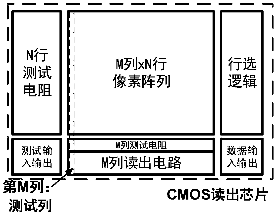
[0063] like image 3As shown, the present application discloses a structural schematic block diagram of a CMOS readout chip, including: M column × N row pixel array, N row test resistor circuit, M column readout circuit, row selection logic circuit, M column test resistor circuit . Test input and output circuits and data input and output circuits; wherein, columns 1 to (M-1) of the M column readout circuits are column-level readout circuits, and the Mth column is a test column.

[0064] like Figure 4 As shown, this embodiment discloses a readout circuit without a MEMS sensor; including: 1 column×N row level test resistor circuit, M column×N row pixel circuit, M column×1 row level test resistor circuit, M Column readout circuit; wherein, the M column readout circuit includes (M-1) column-level readout subcircuits and 1 column test column subcircuit;

[0065] Specifically, the row-level test resistor circuit, the readout circuit, and the column-level test resistor circuit are...


PUM


Abstract

The invention discloses a read-out circuit and a working method thereof, relating to a read-out circuit and a working method thereof. The read-out circuit comprises M columns*N rows of pixel circuits,N rows of row level test resistance circuits, M columns of column level test resistance circuits and M columns of column level read-out circuits, wherein both M and N are natural numbers, M is greater than or equal to 2, and N is greater than or equal to 2, the row level test resistance circuits, the column level test resistance circuits and the columns level read-out circuits are all connected with the pixel circuits, the column level test resistance circuits are connected with the column level read-out circuits, the column level read-out circuits comprise test column secondary circuits, andthe column level read-out circuits are further connected with a current source. Functions of all columns and rows of the whole read-out circuit can be tested without an MEMS sensor, further, more accurate MEMS resistance can be acquired when the MEMS sensor is available, the test result is more accurate, and the test efficiency is improved.

Description

technical field [0001] The invention relates to the field of uncooled infrared detectors, in particular to a readout circuit and a working method thereof. Background technique [0002] In the prior art, the core of an uncooled infrared detector based on a microbolometer is a CMOS (Complementary Metal Oxide Semiconductor) readout circuit and a MEMS (Microelectro Mechanical Systems) sensor. Among them, the CMOS readout circuit completes the signal amplification and readout operation, while the MEMS sensor completes the photoelectric conversion operation. The operation steps in the process are to first process the CMOS readout circuit on the same wafer, and then continue to grow the MEMS sensor structure on the upper end of the circuit. The CMOS readout circuit and the MEMS sensor are integrated into a whole through electrical effective connection, and then a complete detector device can be obtained after packaging and testing steps. [0003] In the development and production...

Claims


Application Information

Patent Timeline
Patent Type & Authority Applications(China)
IPC IPC(8): G01J5/22G01J5/24
CPCG01J5/22G01J5/24
Inventor 施薛优陈光毅
Owner 北京安酷智芯科技有限公司
Why Eureka
Try Eureka