

Method for integrating silicon-based lithium niobate thin film electro-optic modulator arrays
An electro-optic modulator, silicon-based lithium niobate technology, applied in light guides, optics, instruments, etc., can solve the problems of lower conversion rate of electro-optic modulation, low modulation efficiency of doped silicon, high half-wave voltage, etc., to ensure functional effectiveness and stability, improving preparation efficiency, and the effect of ultra-high modulation bandwidth
- Summary
- Abstract
- Description
- Claims
- Application Information
AI Technical Summary
Problems solved by technology
Method used
Image

Examples
Embodiment Construction
[0036] The technical solutions of the present invention will be described in detail below in conjunction with the accompanying drawings and examples, and detailed implementation methods and structures are given, but the scope of protection of the present invention is not limited to the following examples.
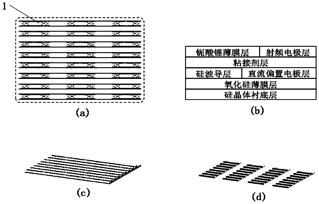
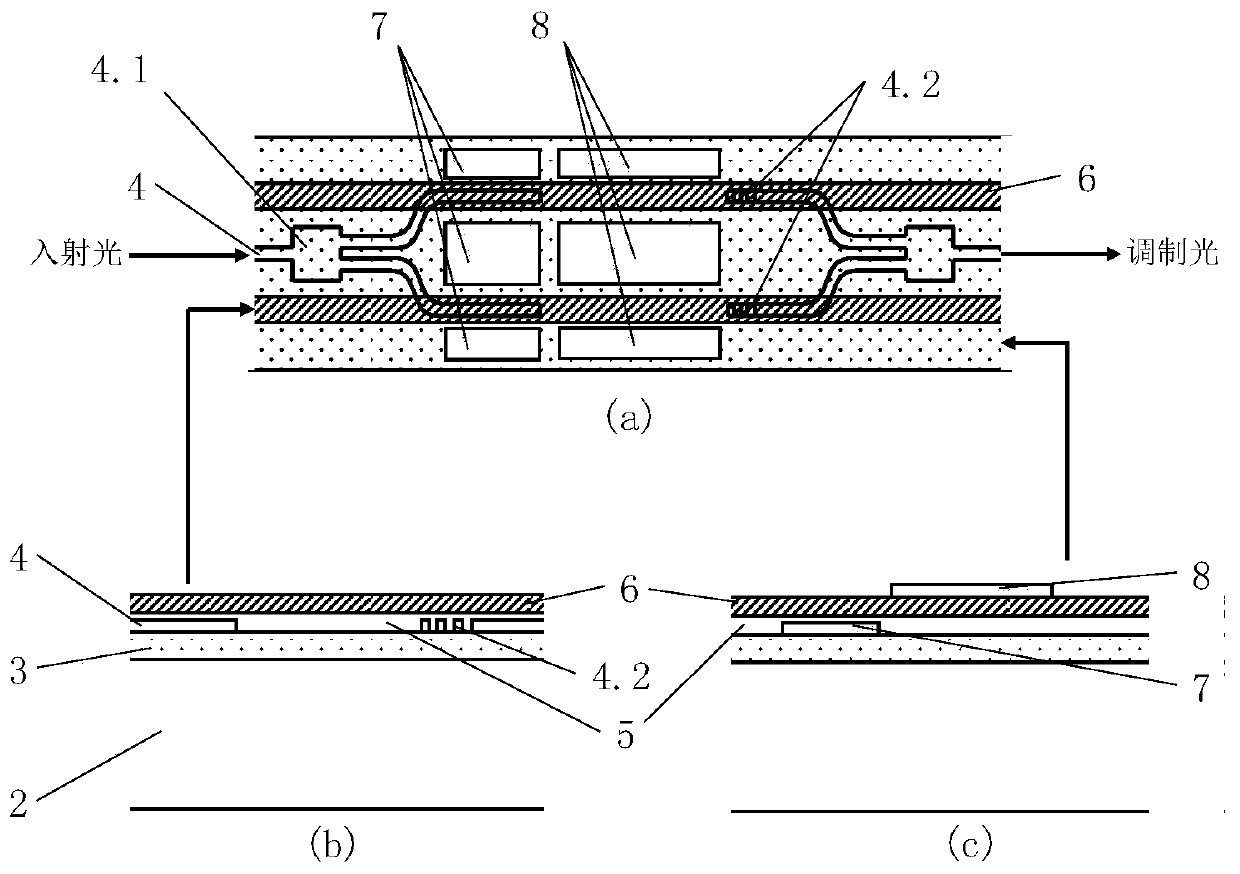
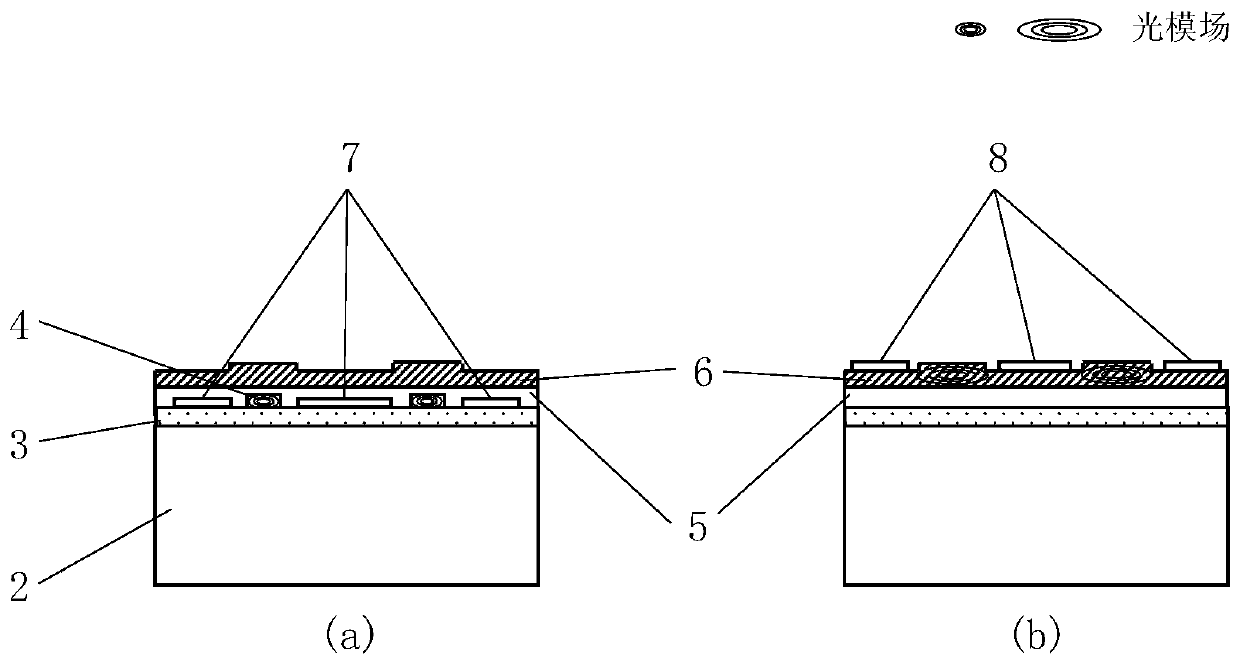
[0037] see figure 1 , figure 1 It is a partial structural schematic diagram of an embodiment of a silicon-based lithium niobate thin-film electro-optic modulator array of the present invention, and the integration method of the silicon-based lithium niobate thin-film electro-optic modulator array of the present invention includes the following steps:
[0038] 1) Forming a silicon oxide thin film layer 3 on a smooth silicon crystal substrate 2 by thermal oxidation;
[0039] 2) Deposit a certain thickness of polysilicon on the silicon oxide thin film layer 3 by chemical vapor deposition (CVD), and then form a plurality of silicon-based lithium niobate thin film electro-opt...
PUM
 Abstract
Description
Claims
Application Information