Methods for growing light emitting devices under ultra-violet illumination

A technology of epitaxial growth and light irradiation, which is used in semiconductor devices, semiconductor/solid-state device manufacturing, electrical components, etc., and can solve problems such as reducing device efficiency, reducing p-type material concentration, and deactivating p-type features.

Active Publication Date: 2019-08-23
LUMILEDS
View PDF6 Cites 0 Cited by
  • Summary
  • Abstract
  • Description
  • Claims
  • Application Information

AI Technical Summary

Problems solved by technology

Hydrogen complexes deactivate the p-type character of magnesium, effectively reducing the effective dopant (and hole) concentration of the p-type material, which reduces the efficiency of the device

Method used


Image

  • Methods for growing light emitting devices under ultra-violet illumination
  • Methods for growing light emitting devices under ultra-violet illumination
  • Methods for growing light emitting devices under ultra-violet illumination

Examples


Embodiment Construction

[0023] It should be understood that the figures and descriptions of the methods for growing light emitting devices under ultraviolet irradiation have been simplified to illustrate elements relevant to a clear understanding, while many other elements found in typical device processes have been removed for the sake of clarity . Those of ordinary skill in the art can recognize that other elements and / or steps are desirable and / or required in implementing the present invention. However, because such elements and steps are well known in the art, and because they would not facilitate a better understanding of the present invention, discussion of such elements and steps is not provided herein.

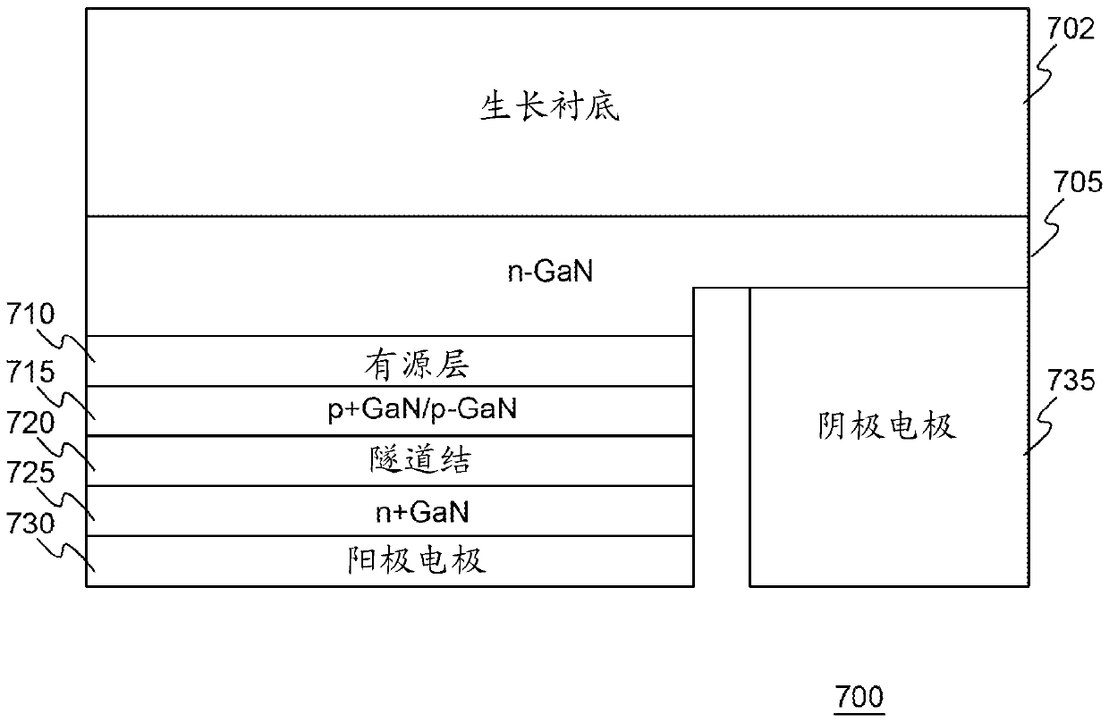
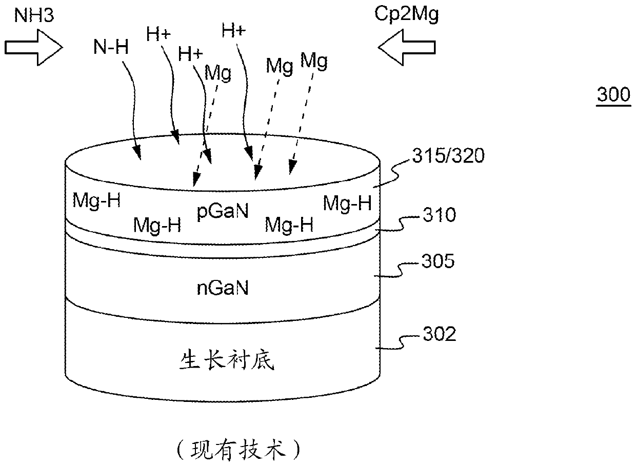
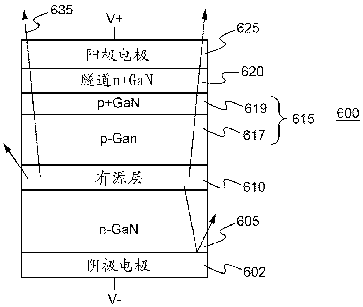
[0024] In a conventional III-nitride light-emitting diode (LED), the n-type layer is first grown on the substrate, followed by the active layer (or light-emitting layer) and the p-type layer. As used herein, the term layer refers to at least one of the identified layers, for example, a p-typ...


PUM


Abstract

Described herein are methods for growing light emitting devices under ultra-violet (UV) illumination. A method includes growing a III-nitride n-type layer over a III-nitride p-type layer under UV illumination. Another method includes growing a light emitting device structure on a growth substrate and growing a tunnel junction on the light emitting device structure, where certain layers are grown under UV illumination. Another method includes forming a III-nitride tunnel junction n-type layer over the III-nitride p-type layer to form a tunnel junction light emitting diode. A surface of the III-nitride tunnel junction n-type layer is done under illumination during an initial period and a remainder of the formation is completed absent illumination. The UV light has photon energy higher than the III-nitride p-type layer's band gap energy. The UV illumination inhibits formation of Mg-H complexes within the III-nitride p-type layer resulting from hydrogen present in a deposition chamber.

Description

[0001] Cross References to Related Applications [0002] This application claims U.S. Provisional Application No. 62 / 414,612, filed October 28, 2016, European Provisional Application No. 16204234.5, filed December 15, 2016, and U.S. Non-Provisional Application No. 15 / 793,723, the contents of which are hereby incorporated by reference as if fully set forth. technical field [0003] The present application relates to light emitting devices. Background technique [0004] Semiconductor light emitting devices including light emitting diodes (LEDs), resonant cavity light emitting diodes (RCLEDs), vertical cavity surface emitting lasers (VCSELs) and edge emitting lasers are the most efficient light sources currently available. Materials systems currently of interest in the fabrication of high-brightness light-emitting devices capable of operating across the visible spectrum include III-V semiconductors, in particular binary, ternary and quaternary alloys of gallium, aluminum, ind...

Claims


Application Information

Patent Timeline
IPC IPC(8): H01L33/00H01L21/02H01L21/268H01L33/32
CPCC23C16/303C23C16/482H01L21/02458H01L21/0254H01L21/02579H01L21/0262H01L33/0062H01L33/0075H01L33/0095H01L33/025H01L33/32H01L21/2686H01L33/007H01L33/0008H01L33/06
Inventor T.伊施卡瓦I.维尔德森E.C.尼尔森P.德布
Owner LUMILEDS
Why Eureka
Try Eureka