
Electric field assisted atomic force microscope nano-etching method

An atomic force microscope and nanotechnology, applied in the field of nanoprocessing, can solve the problems of expensive diamond probes, single diamond scribed shape, and easy torsion of cantilever beams, etc., and achieve flexible processing methods, good isotropic consistency, and low prices Effect

Inactive Publication Date: 2019-08-27
刘增磊
View PDF0 Cites 0 Cited by
  • Summary
  • Abstract
  • Description
  • Claims
  • Application Information

AI Technical Summary

Problems solved by technology

[0003] 1. Diamond probes are expensive
[0004] 2. Diamond cutting relies on the action of mechanical force, which will cause the position of the assembled nanomaterials to move during the cutting process
[0005] 3. The shape of the diamond scribe is relatively simple
Since the diamond probe has a slender cantilever beam structure, it is suitable for marking along the axis of the cantilever beam of the diamond probe; when marking sideways, the cantilever beam is prone to twist, which affects the marking effect

Method used


Image

  • Electric field assisted atomic force microscope nano-etching method
  • Electric field assisted atomic force microscope nano-etching method
  • Electric field assisted atomic force microscope nano-etching method

Examples


Embodiment Construction

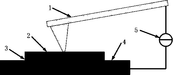
[0018] A programmable current source 5 is applied to the sample 2 and the AFM conductive probe 1 through the power interface provided by the atomic force microscope itself. In principle, the direction of the current does not affect the processing effect. However, considering that the tip is connected to the anode, the discharge voltage is lower. Therefore, the AFM probe is connected to the anode and the sample is connected to the cathode.

[0019] Through the scanning function of the atomic force microscope, the shape of the sample is scanned and the processing position is selected.

[0020] Set the current parameters on the programmable current source 5 . Including current magnitude, duration, current waveform, etc.

[0021] Set the AFM to work in contact mode, so that the AFM probe is in contact with the sample. And the contact force between the probe and the sample is controlled by the Deflection setpoint parameter.

[0022] Plan the trajectory of the probe, and set th...


PUM


Abstract

The invention discloses a method for realizing AFM (Atomic Force Microscopy) nano-etching by applying current. Certain current is applied to an AFM needle tip and a substrate, the magnitude of the current is controlled, and due to the fact that large contact resistance exists between the needle tip and the sample, certain joule heat is generated, and etching is formed on the substrate. The methodcan be used for the operations of processing nano-groove marks, cutting nano-materials and the like.

Description

technical field [0001] The invention relates to the field of nano-processing, specifically a method of applying an electric current between an atomic force microscope (AFM) probe and a substrate, and making the probe tip move on the surface of the substrate to form nano-scratches through Joule heat, thereby realizing nano-processing. Methods of etching and cutting. Background technique [0002] Nano-devices are electronic devices composed of nano-materials, such as various gas sensors, biosensors, field-effect transistors, and so on. Nano-devices have excellent properties, such as the Coulomb blocking effect and so on. However, nano-devices have not yet been widely used. This is because there are still various problems in the processing and manufacturing of nano-devices. Such as nano-welding, nano-assembly, nano-cutting and other issues. Among them, nano-cutting is to cut nano-materials into specific sizes and shapes according to needs. At present, diamond probes can be...

Claims


Application Information

Patent Timeline
Patent Type & Authority Applications(China)
IPC IPC(8): B81C1/00
CPCB81C1/00492B81C1/00626B81C2201/0146
Inventor 刘增磊高爱莲
Owner 刘增磊
Learn More