Integrated embedded miniaturized phased array monitoring and calibration network based on PCB lamination technology

A built-in, phased array technology, applied in transmitter monitoring, radio wave measurement systems, instruments, etc., can solve the problems of space occupation, weight and cost, poor network integrity, and difficult integration, etc., and achieve low processing difficulty, Easy integration and low cost effect

Active Publication Date: 2019-08-27
CNGC INST NO 206 OF CHINA ARMS IND GRP
View PDF8 Cites 6 Cited by
  • Summary
  • Abstract
  • Description
  • Claims
  • Application Information

AI Technical Summary

Problems solved by technology

A large number of cables or connectors are required between the two parts, which takes up ad...

Method used


Image

  • Integrated embedded miniaturized phased array monitoring and calibration network based on PCB lamination technology
  • Integrated embedded miniaturized phased array monitoring and calibration network based on PCB lamination technology
  • Integrated embedded miniaturized phased array monitoring and calibration network based on PCB lamination technology

Examples


Embodiment Construction

[0028] Now in conjunction with embodiment, accompanying drawing, the present invention will be further described:

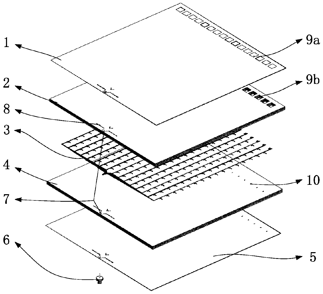
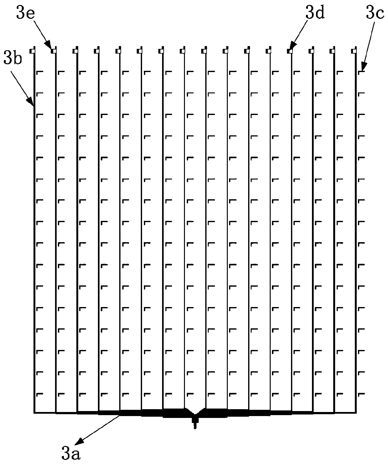
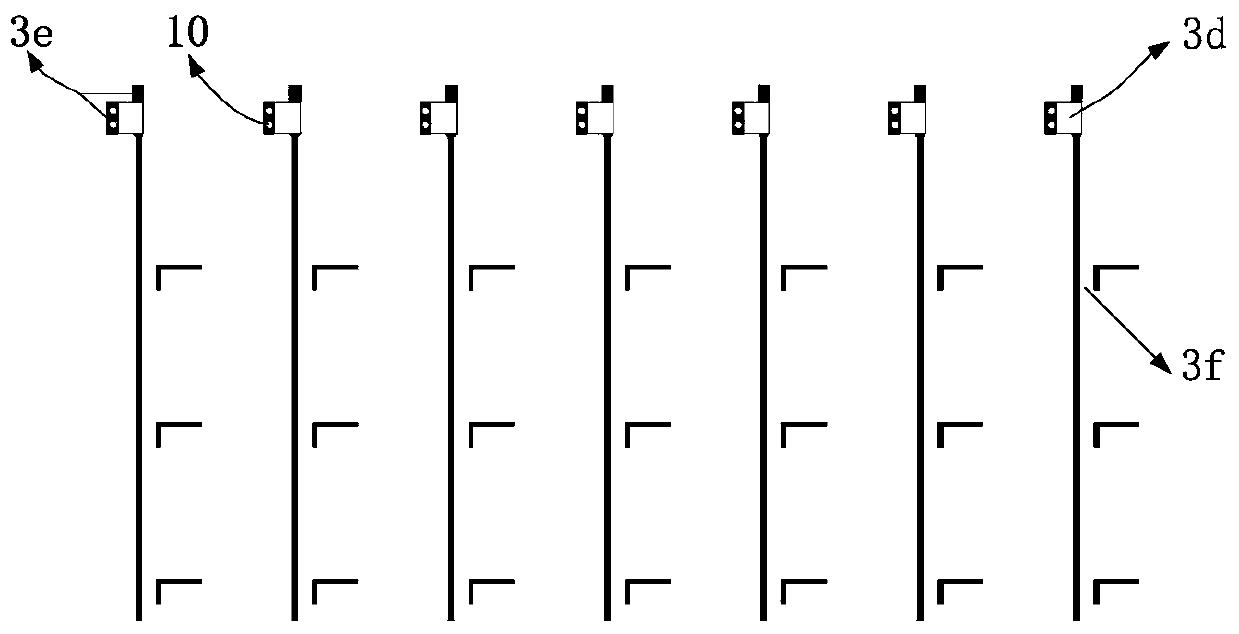
[0029] The integrated embedded miniaturized phased array monitoring and calibration network based on laminated PCB technology adopts a laminated stripline structure, including an upper metal floor, a lower metal floor, a high-frequency dielectric board, a stripline power divider, and a Shaped transmission lines, calibration signal coupling structures, microstrip transmission lines, terminated attenuators and SMP connectors. The entire network is composed of two layers of dielectric boards. The material of the multi-layer board is Taconic TSM-DS3 high-frequency dielectric substrate with a dielectric constant εr=3. The boards are crimped by a prepreg film. Taconic FR-27 with constant εr = 2.7.

[0030] The main body of the monitoring calibration network is a closed stripline structure. The signal output / input port is an SMP connector. The probe of the connector i...


PUM


Abstract

The invention relates to an integrated embedded miniaturized phased array monitoring and calibration network based on a PCB lamination technology. The integrated embedded miniaturized phased array monitoring and calibration network comprises a miniaturized strip line power divider, a metalized isolated via hole array, a calibration signal coupling structure, a strip line signal transmission structure, a micro-strip transmission line, a terminal matching attenuator and a feed SMP connector. The calibration network is built by the PCB lamination technology; the strip line power divider, the metalized isolated via hole array, the calibration signal transmission line, the terminal matching structure and the like together form a whole array surface calibration signal transceiving distribution network; and real-time monitoring of signals received and transmitted on the array surface of a phased-array antenna in a multi-layer micro-strip form is completed. The monitoring and calibration network has the characteristics of compact structure, low profile, low cost, easiness in processing, full integration and the like, can meet the use requirements of the whole Ku frequency band of 12-18GHz,and is very suitable for an application to a Ku waveband phased array antenna system.

Description

technical field [0001] The invention relates to an integrated embedded miniaturized phased array monitoring and calibration network based on laminated PCB technology, which can be applied to a Ku-band broadband phased array system and belongs to the technical field of wireless communication system antennas. Background technique [0002] With the rapid development of radar sensors and satellite communication systems, active phased arrays with fast beam scanning and adaptive beamforming will become their mainstream hardware solutions. In the application process of active phased array, as the ambient temperature changes, there will be certain dynamic fluctuations in the channel transmission characteristics (amplitude and phase), and the inconsistency between the amplitude and phase of the channels will cause the array to appear such as the decrease of radiation efficiency. , sidelobe level elevation, beam pointing deviation and a series of problems. In order to ensure the norm...

Claims


Application Information

Patent Timeline
IPC IPC(8): G01S7/40H01Q3/26H04B17/12
CPCG01S7/4008H01Q3/267H04B17/12
Inventor 王元源郑慕昭华根瑞李宁王敏
Owner CNGC INST NO 206 OF CHINA ARMS IND GRP
Why Eureka
Try Eureka