Mesa PIN passivation structure, photodiode and preparation method of photodiode

A photodiode, mesa technology, applied in the field of optical communication, to achieve the effect of short growth time and improved reliability

Active Publication Date: 2019-08-27
XIAMEN SANAN INTEGRATED CIRCUIT
View PDF12 Cites 6 Cited by
  • Summary
  • Abstract
  • Description
  • Claims
  • Application Information

AI Technical Summary

Problems solved by technology

[0006] One of the purposes of the present invention is to provide a passivation structure and a photodiode of a mesa PIN, which can not only solve the problem of electric leakage in the side passivation structure of the existing mesa PIN, improve chip performance, but also have simple process and good yield

Method used


Image

  • Mesa PIN passivation structure, photodiode and preparation method of photodiode
  • Mesa PIN passivation structure, photodiode and preparation method of photodiode

Examples


Embodiment Construction

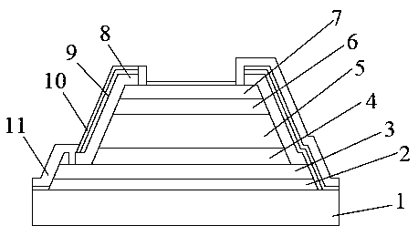
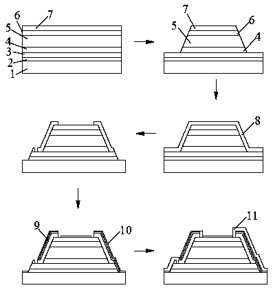
[0036] The present invention will be further described in detail below in conjunction with the accompanying drawings and specific embodiments. What the present invention discloses is a passivation structure of a PIN mesa, which has P-type, I-type and N-type semiconductor layers, and the P-type, I-type and N-type semiconductor layers constitute a stepped layer mesa, wherein the I-type semiconductor layer is An InGaAs absorption layer 5, and an Fe-doped semi-insulating InGaAs layer 8 is grown on the side wall of the InGaAs absorption layer 5 . Fe-doped semi-insulating InGaAs is used as the passivation layer, which belongs to homoepitaxy, and the interface defect density of the I layer (type I semiconductor layer) is low, which can prevent leakage.

[0037] Further, a secondary passivation layer 9 and an anti-reflection film 10 are sequentially grown on the Fe-doped semi-insulating InGaAs layer 8, the secondary passivation layer is a BCB or PI layer, and the anti-reflection film ...


PUM


Abstract

The invention discloses a mesa PIN passivation structure. The mesa PIN passivation structure is provided with P-type, I-type and N-type semiconductor layers which form a step layer mesa, wherein the I-type semiconductor layer is an InGaAs absorption layer; and a Fe-doped semi-insulating InGaAs layer grows on a side wall of the InGaAs absorption layer. The invention further discloses a high-speed mesa InGaAs photodiode and a preparation method thereof. The problem of electric leakage of an existing mesa PIN side surface passivation structure can be solved, and the chip performance is improved;and moreover, the process is simple, and the rate of finished products is high.

Description

technical field [0001] The invention belongs to the technical field of optical communication, and in particular relates to a mesa PIN passivation structure, a photodiode and a preparation method thereof. Background technique [0002] A photodiode (Photo-Diode) is a semiconductor device composed of a PN junction with unidirectional conductivity. The photodiode works under the action of reverse voltage, and the current generated under the light of general illuminance is called photocurrent. If a load is connected to the external circuit, an electrical signal is obtained on the load, and this electrical signal changes correspondingly with the change of light. Among them, high-speed InGaAs PD is the core component in the field of optical communication. At present, PDs above 10G generally adopt a mesa PIN structure. The mesa PIN structure is formed by corrosion method. Since the PN is exposed and the drain electrode on the side of the device is large, it is necessary to use BCB...

Claims


Application Information

Patent Timeline
Patent Type & Authority Applications(China)
IPC IPC(8): H01L31/0352H01L31/032H01L31/0216H01L31/18
CPCH01L31/02161H01L31/0322H01L31/035281H01L31/1876Y02E10/541
Inventor 张江勇林科闯林峰
Owner XIAMEN SANAN INTEGRATED CIRCUIT
Why Eureka
Try Eureka