A flat panel detector and its manufacturing method

A technology of flat panel detector and manufacturing method, which is applied in the field of photoelectric detection, can solve the problems affecting the detection accuracy of the detector, uneven distribution of dark current, etc., and achieve the effect of improving uniformity and detection accuracy

Active Publication Date: 2021-08-06
BOE TECH GRP CO LTD +1
View PDF0 Cites 0 Cited by
  • Summary
  • Abstract
  • Description
  • Claims
  • Application Information

AI Technical Summary

Problems solved by technology

[0004] The embodiment of the present invention provides a flat panel detector and its manufacturing method to solve the problem that the dark current distribution of the existing flat panel detector is uneven and affects the detection accuracy of the detector

Method used


Image

  • A flat panel detector and its manufacturing method
  • A flat panel detector and its manufacturing method
  • A flat panel detector and its manufacturing method

Examples


Embodiment Construction

[0040] The following will clearly and completely describe the technical solutions in the embodiments of the present invention with reference to the accompanying drawings in the embodiments of the present invention. Obviously, the described embodiments are some of the embodiments of the present invention, but not all of them. Based on the embodiments of the present invention, all other embodiments obtained by persons of ordinary skill in the art without creative efforts fall within the protection scope of the present invention.

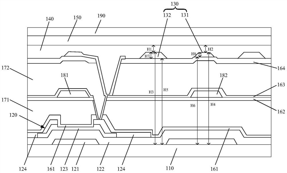
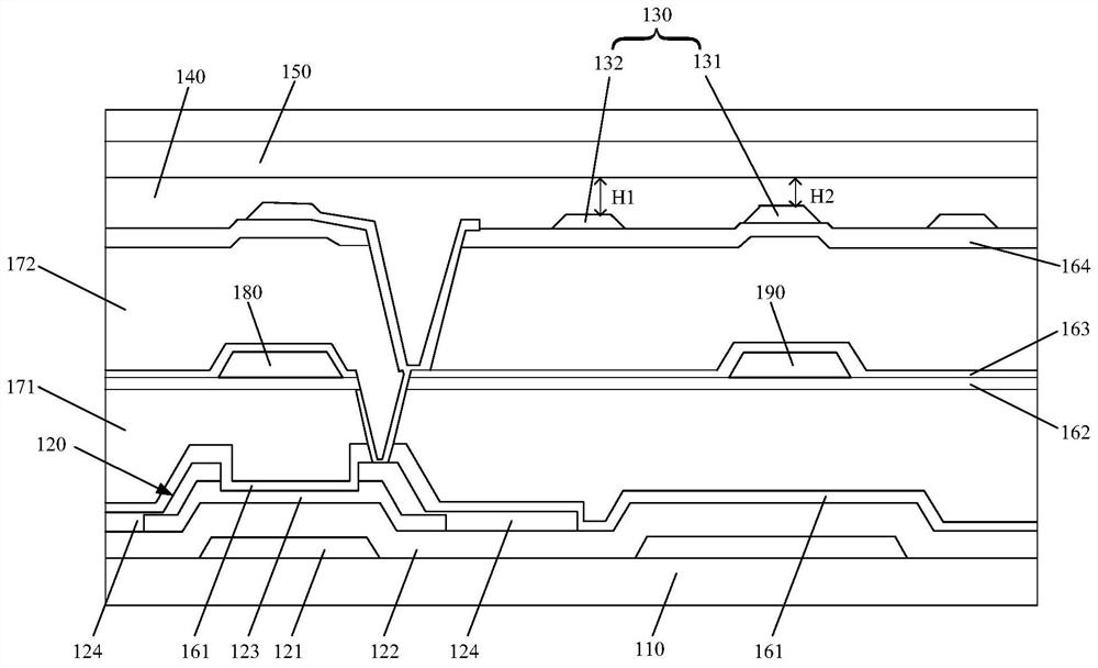
[0041] The invention provides a flat panel detector.

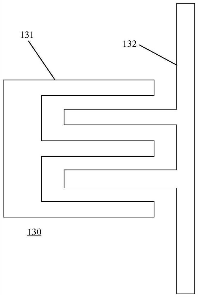
[0042] Such as figure 1 As shown, the flat panel detector includes a base substrate 110 , a thin film transistor 120 , a sensor (Sense) electrode 131 , a bias electrode (Bias) 132 , an insulating layer 140 and a semiconductor layer 150 .

[0043] The base substrate 110 in this embodiment may be a glass substrate or a substrate made of organic materials, for details, reference may be made to relate...


PUM


Abstract

The invention provides a flat panel detector and a manufacturing method thereof. The flat panel detector includes a base substrate, a sensing electrode, a bias electrode and an insulating layer, the sensing electrode and the bias electrode are located on the base substrate, and the insulating layer is located between the sensing electrode and the bias electrode. The electrode is far away from the side of the base substrate, and the thickness difference between the region of the insulating layer corresponding to the sensing electrode and the region of the insulating layer corresponding to the bias electrode is not greater than a preset threshold. In the embodiment of the present invention, when a sufficiently high voltage is applied on the insulating layer and turned on, since its thickness is relatively uniform, the dark current generated by the sensing electrode and the bias electrode under the insulating layer is also relatively uniform, thus improving the flat panel detector. The uniformity of the dark current distribution helps to improve the detection accuracy of the flat panel detector.

Description

technical field [0001] The invention relates to the technical field of photoelectric detection, in particular to a flat panel detector and a manufacturing method thereof. Background technique [0002] MSM (Metal-Semiconductor-Metal) type X-ray (X-ray, also known as X-ray) detector refers to a metal-semiconductor-metal interdigitated electrode, and a polymer is filled between the metal interdigitated electrode and the semiconductor layer Detectors with imide (PI) insulating layers. Under the condition of light, the semiconductor of the detector receives light, generates charges inside, and the resistance drops significantly, thereby converting the light signal into an electrical signal through the photovoltaic effect. At this time, most of the external bias voltage is applied to the PI layer with high resistance. On the other hand, when the voltage is high enough, the PI thin film can be turned on through the F-N tunneling effect of electrons, and the electrical signal gener...

Claims


Application Information

Patent Timeline
Patent Type & Authority Patents(China)
IPC IPC(8): H01L31/119H01L31/20H01L27/144
CPCH01L31/119H01L31/202H01L27/1443H01L27/14603H01L31/085H01L31/09H01L31/0224H01L31/022408
Inventor 梁魁刘大力陈江博张硕李凡李达
Owner BOE TECH GRP CO LTD
Why Eureka
Try Eureka