Method and device for optimizing thickness of absorption layer of far infrared blocking impurity band detector

A technology for blocking impurities and optimizing methods, which is applied in photometry, instruments, calculations, etc. using electric radiation detectors, and can solve the problem of reduced photoelectric conversion efficiency of far-infrared radiation, reduced photogenerated carrier transport efficiency, and detector production costs. Increase and other problems, to avoid repeated test pieces, optimize the thickness of the absorbing layer, and reduce the cost of research and development

Active Publication Date: 2019-08-30
上海微波技术研究所(中国电子科技集团公司第五十研究所)
View PDF13 Cites 4 Cited by
  • Summary
  • Abstract
  • Description
  • Claims
  • Application Information

AI Technical Summary

Problems solved by technology

The thickness of the absorbing layer has a significant impact on the cost performance of BIB detectors. On the one hand, if the thickness of the absorbing layer is too thin, the photoelectric conversion efficiency of far-infrared radiation will decrease; on the other hand, if the thickness of the absorbing layer is too thick, the transport efficiency of photogenerated carriers will decrease. will decrease and the production c

Method used


Image

  • Method and device for optimizing thickness of absorption layer of far infrared blocking impurity band detector
  • Method and device for optimizing thickness of absorption layer of far infrared blocking impurity band detector
  • Method and device for optimizing thickness of absorption layer of far infrared blocking impurity band detector

Examples


Embodiment Construction

[0057] The present invention will be described in detail below in conjunction with specific embodiments. The following examples will help those skilled in the art to further understand the present invention, but do not limit the present invention in any form. It should be noted that those skilled in the art can make several changes and modifications without departing from the concept of the present invention.

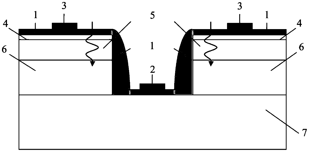
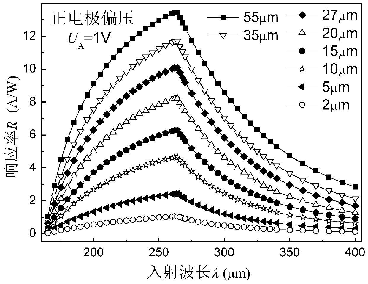
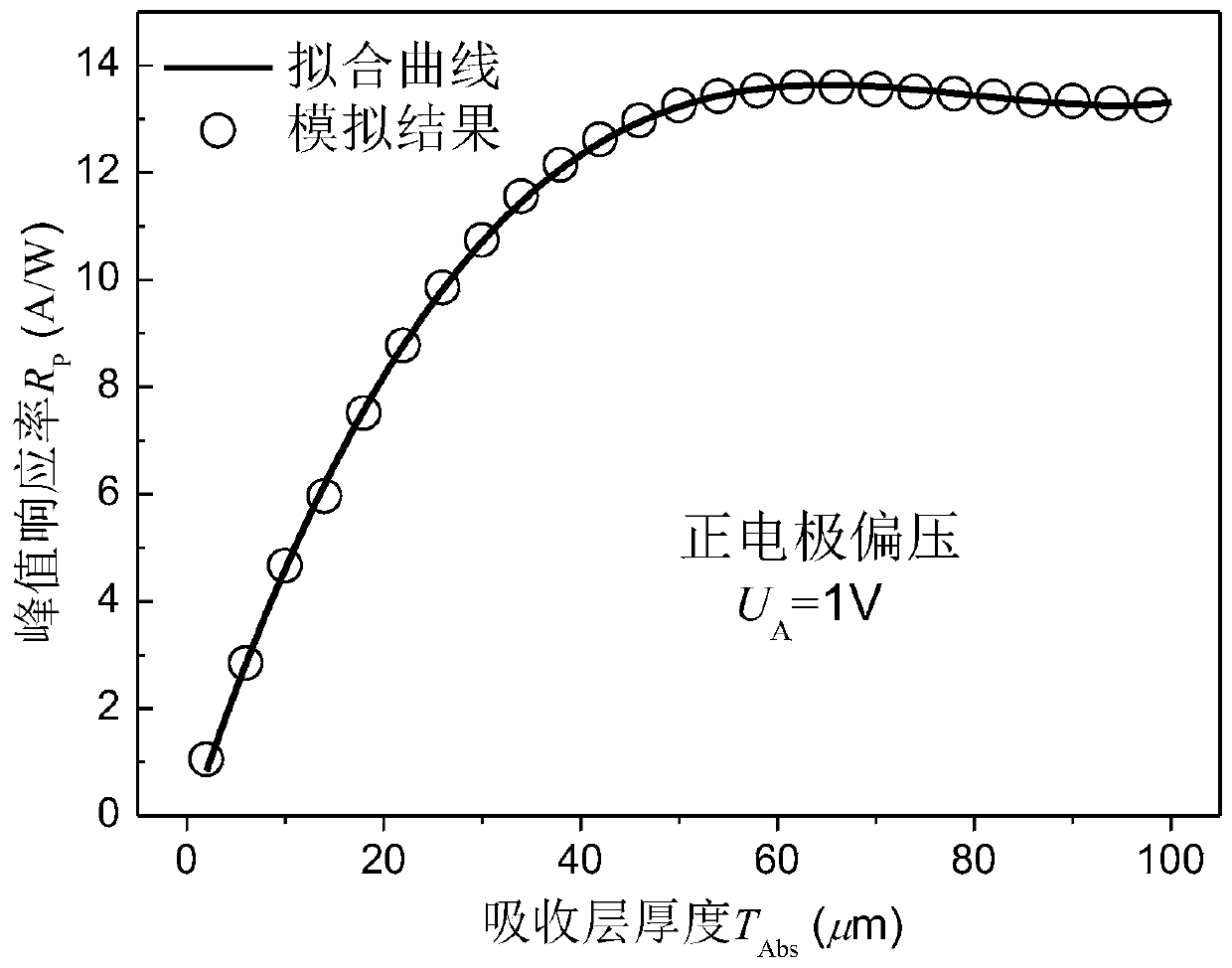
[0058] Such as Figure 1 to Figure 6 As shown, according to the method for optimizing far-infrared blocking impurity band (BIB) detector absorbing layer thickness provided by the present invention, the method obtains BIB detector peak responsivity and production cost with absorbing layer thickness variation by numerical simulation and data fitting law. In order to obtain the highest cost performance of the detector, the quotient of the peak responsivity and the production cost of the detector is defined as the cost performance factor of the detector. The optimal thick...


PUM


Abstract

The invention provides a method and a device for optimizing the thickness of an absorption layer of a far infrared blocking impurity band detector, and the method comprises the following steps: obtaining parameters of a physical model of the blocking impurity band detector, and constructing a numerical model of the blocking impurity band detector; according to the numerical model, obtaining a curve of change of the response rate R of the blocking impurity band detector along with the incident wave length; changing the thickness of an absorption layer in the numerical model to obtain a corresponding spectral response rate curve, and obtaining a peak wavelength P of the spectral response rate curve; obtaining a functional expression of a curve which fits the change of the peak response rateRP along with the thickness Tabs of the absorption layer under the bias voltage UF of the positive electrode; obtaining a functional expression of a curve which fits and blocks the change of the impurity band detector production cost Cm along with the absorption layer thickness Tabs; and obtaining the optimal absorption layer thickness according to the obtained functional expression. The method has the advantages that the functional expressions of cost performance factors of the detector with respect to different absorption layer thicknesses are obtained through numerical simulation and data fitting, and the optimal absorption layer thickness is extracted according to the functional expressions.

Description

technical field [0001] The present invention relates to semiconductor photodetector technology, in particular to a method and device for optimizing the thickness of an absorbing layer of a far-infrared blocking impurity band detector. Background technique [0002] Far-infrared rays generally refer to electromagnetic waves with a wavelength between 25 microns and 500 microns. Far-infrared rays have obvious penetrating ability and fingerprint characteristics, so they have broad application prospects in the fields of astronomical observation, atmospheric monitoring and contraband detection. In the field of astronomical observation, almost all planets and cosmic dust have obvious characteristic absorption peaks in the far-infrared band, and gaseous nebulae can emit far-infrared rays through the internal rotation and vibration of molecules, so the use of far-infrared detectors can achieve high-performance deep space probing. In the field of atmospheric monitoring, compared with...

Claims


Application Information

Patent Timeline
IPC IPC(8): G06F17/50G01J1/42
CPCG01J1/42G06F30/20Y02P70/50
Inventor 王晓东陈雨璐王兵兵张传胜童武林胡永山张皓星俞旭辉
Owner 上海微波技术研究所(中国电子科技集团公司第五十研究所)
Why Eureka
Try Eureka