
Wafer level packaging structure and packaging method of floodlight module

A technology of wafer-level packaging and flood lighting, which is applied in the direction of electrical components, electrical solid-state devices, circuits, etc., and can solve the problems that cannot meet the needs of miniaturization and miniaturization of products in the electronics industry, large device size, and low device volume requirements, etc. problems, to achieve the effect of good consistency, high alignment accuracy, and excellent optical performance

Active Publication Date: 2019-08-30
华天慧创科技(西安)有限公司
View PDF10 Cites 3 Cited by
  • Summary
  • Abstract
  • Description
  • Claims
  • Application Information

AI Technical Summary

Problems solved by technology

[0002] With the maturity of TOF (time of flight) and structured light 3D sensing technology, and the rapid development of the 3D camera industry, the ordinary floodlight module is far from meeting the market demand. For example, the camera module and the floodlight module work together. It has been widely used in 3D reconstruction, face recognition and other fields, but limited by the manufacturing process of existing module production, there is still room for improvement in product consistency and alignment accuracy.
[0003] The processing technology of traditional optical devices does not have high requirements on the volume of the device, and the size of the device is usually large, which can no longer meet the needs of miniaturization and miniaturization of products in the electronics industry.

Method used


Image

  • Wafer level packaging structure and packaging method of floodlight module
  • Wafer level packaging structure and packaging method of floodlight module
  • Wafer level packaging structure and packaging method of floodlight module

Examples


Embodiment 1

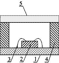
[0033] Such as figure 1 As shown, a wafer-level packaging structure of a floodlighting module in this embodiment includes a substrate 1, a functional chip 2, spacers 4, and optical components 5; wherein, the substrate 1 is a ceramic substrate, and the substrate 1 is It has at least one pair of positioning marks (not shown); the functional chip 2 is arranged on the surface of the substrate, the functional chip 2 is a vertical cavity surface emitting laser, and the surface of the functional chip 2 is electrically connected to the surface of the substrate 1 through a metal wire 3; the functional chip 2 The peripheral substrate is provided with a spacer 4, the upper end of the spacer 4 is higher than the functional chip 2; the optical component 5 is arranged above the functional chip 2, and the two ends of the optical component 5 are respectively connected to the spacer 4 on the periphery of the functional chip 2. The top end of the optical component 5 and the spacer 4 jointly for...

Embodiment 2

[0038] A wafer-level packaging method for a floodlighting module, comprising the following steps:

[0039] 1. See figure 2 , providing a clean substrate 1 having at least one pair of positioning marks (not shown).

[0040] Two, see image 3 , integrating multiple functional chips 2 onto the substrate through a die bond process.

[0041] Three, see Figure 4 , using a wire bonding (wire bond) process to realize the electrical connection between the functional chip 2 and the surface of the substrate 1 through the metal wire 3 .

[0042] 4. Apply glue dispensing process to coat glue layer A (not shown) on the surface of the substrate between multiple functional chips 2;

[0043] 5. Use a photolithography machine to complete the alignment of the spacer 4 and the substrate 1 through the semiconductor back side alignment (Back Side Alignment). After the alignment is completed, the lower end of the spacer 4 is in contact with the adhesive layer A; lock the substrate 1 and The s...


PUM


Abstract

The invention provides a wafer level packaging structure and a packaging method of a floodlight module. The wafer level packaging structure comprises a structure substrate, a functional chip, a spacerand an optical component; the functional chip is arranged at the surface of the substrate, the surface of the functional chip is electrically connected with the surface of the substrate through a metal wire; the substrate at the periphery of the functional chip is provided with the spacer, and the upper end of the spacer is higher than the functional chip; the optical component is arranged at theupper portion of the functional chip, two ends of the optical component are respectively connected with the top end of the spacer on the periphery of the functional chip, the optical component and the spacer jointly form a cavity structure, and the functional chip is located at the lower portion of the cavity structure. The optical component is formed by adopting a photoetching machine for imprinting, the alignment precision of the optical component with the substrate is high, and the finished product yield is high; the floodlight module adopts a wafer-level process, the optical component andthe substrate are pressed together by the wafer-level process, and then the optical component and the substrate are cut into single modules, so that the floodlight module has the characteristics of asmall size, a low height, good consistency and the like.

Description

technical field [0001] The invention relates to the field of photoelectric modules, in particular to a wafer-level packaging structure and packaging method of a floodlighting module. Background technique [0002] With the maturity of TOF (time of flight) and structured light 3D sensing technology, and the rapid development of the 3D camera industry, the ordinary floodlight module is far from meeting the market demand. For example, the camera module and the floodlight module work together. It has been widely used in 3D reconstruction, face recognition and other fields, but limited by the manufacturing process of existing module production, there is still room for improvement in product consistency and alignment accuracy. [0003] Traditional optical device processing technology does not have high requirements on the volume of the device, and the size of the device is usually large, which can no longer meet the needs of the miniaturization and miniaturization of products in th...

Claims


Application Information

Patent Timeline
Patent Type & Authority Applications(China)
IPC IPC(8): H01L23/31H01L23/544H01L21/56
CPCH01L21/56H01L23/3107H01L23/3114H01L23/544H01L2224/48091H01L2224/97H01L2924/16195H01L2924/00014
Inventor 李卫士杨超
Owner 华天慧创科技(西安)有限公司
Learn More