

Method for preparing gold-silver selenide-lead phosphate heterojunction nano-film
A nano-film and heterojunction technology, applied in the fields of electrochemistry and nano-film materials, can solve the problems of cumbersome preparation process, incompatible with the development of green chemistry, and large consumption of reagents, and achieve simple preparation process, easy large-scale production, The effect of small consumption of reagents
- Summary
- Abstract
- Description
- Claims
- Application Information
AI Technical Summary
Problems solved by technology
Method used
Image

Examples
Embodiment 1
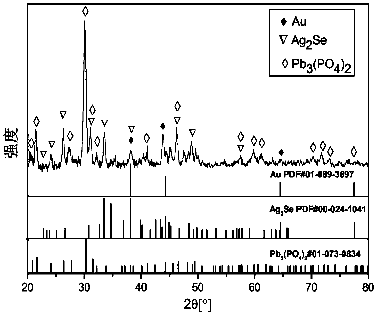
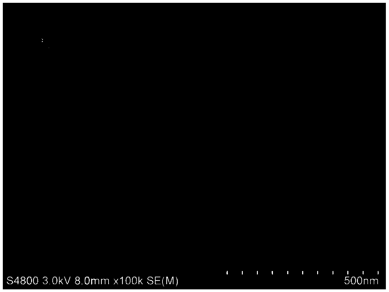
[0018] This embodiment is used to illustrate the present invention Au-Ag 2 Se-Pb 3 (PO 4 ) 2 Characterization analysis of nano-heterojunction films and their morphology and structure.
[0019] (1) Clean the pre-cut 1cm×3cm ITO conductive glass electrode with analytical pure acetone, absolute ethanol and secondary water for 20 minutes respectively, and after drying, use a multimeter to measure the conductive surface before use.
[0020] (2) Measure 1 mL of Pb(NO 3 ) 2 solution, 1.5mL EDTA solution with a concentration of 0.2mol / L, 3.5mL SeO with a concentration of 0.01mol / L 2 solution, 3 mL of Na with a concentration of 1.25 mol / L 2 SO 4 The solution was placed in a 20mL beaker and mixed evenly to prepare the bottom solution for electrodepositing PbSe thin film.
[0021] (3) set up a three-electrode system in the bottom solution of the electrodeposited PbSe film made in step (2), wherein, the working electrode is the conductive glass electrode made in the step (1), and ...
Embodiment 2
[0028] (1) Clean the pre-cut 1cm×3cm ITO conductive glass electrode with analytical pure acetone, absolute ethanol and secondary water for 20 minutes respectively, and after drying, use a multimeter to measure the conductive surface before use.
[0029] (2) Measure 1 mL of Pb(NO 3 ) 2 solution, 1.5mL EDTA solution with a concentration of 0.2mol / L, 3.5mL SeO with a concentration of 0.01mol / L 2 solution, 3 mL of Na with a concentration of 1.25 mol / L 2 SO 4 The solution was placed in a 20mL beaker and mixed evenly to prepare the bottom solution for electrodepositing PbSe thin film.
[0030] (3) set up a three-electrode system in the bottom solution of the electrodeposited PbSe film made in step (2), wherein, the working electrode is the conductive glass electrode made in the step (1), and the counter electrode is a Pt electrode, and the reference The electrode is an Ag / AgCl electrode, and the electrodeposition is carried out by cyclic voltammetry. The potential scanning range...
Embodiment 3
[0035] (1) Clean the pre-cut 1cm×3cm ITO conductive glass electrode with analytical pure acetone, absolute ethanol and secondary water for 20 minutes respectively, and after drying, use a multimeter to measure the conductive surface before use.
[0036] (2) Measure 1 mL of Pb(NO 3 ) 2 solution, 1.5mL EDTA solution with a concentration of 0.2mol / L, 3.5mL SeO with a concentration of 0.01mol / L 2 solution, 3 mL of Na with a concentration of 1.25 mol / L 2 SO 4 The solution was placed in a 20mL beaker and mixed evenly to prepare the bottom solution for electrodepositing PbSe thin film.
[0037] (3) set up a three-electrode system in the bottom solution of the electrodeposited PbSe film made in step (2), wherein, the working electrode is the conductive glass electrode made in the step (1), and the counter electrode is a Pt electrode, and the reference The electrode is an Ag / AgCl electrode, and the electrodeposition is carried out by cyclic voltammetry. The potential scanning range...
PUM
 Abstract
Description
Claims
Application Information