Perovskite polycrystalline film printing preparation method
A technology of perovskite and perovskite precursors, which is applied in semiconductor/solid-state device manufacturing, semiconductor devices, electrical components, etc., can solve the problems of uncontrollable crystallization process and poor scalability of material systems, and achieve industrialization development. The effect of reducing energy consumption
- Summary
- Abstract
- Description
- Claims
- Application Information
AI Technical Summary
Problems solved by technology
Method used
Image
Examples
Embodiment 1
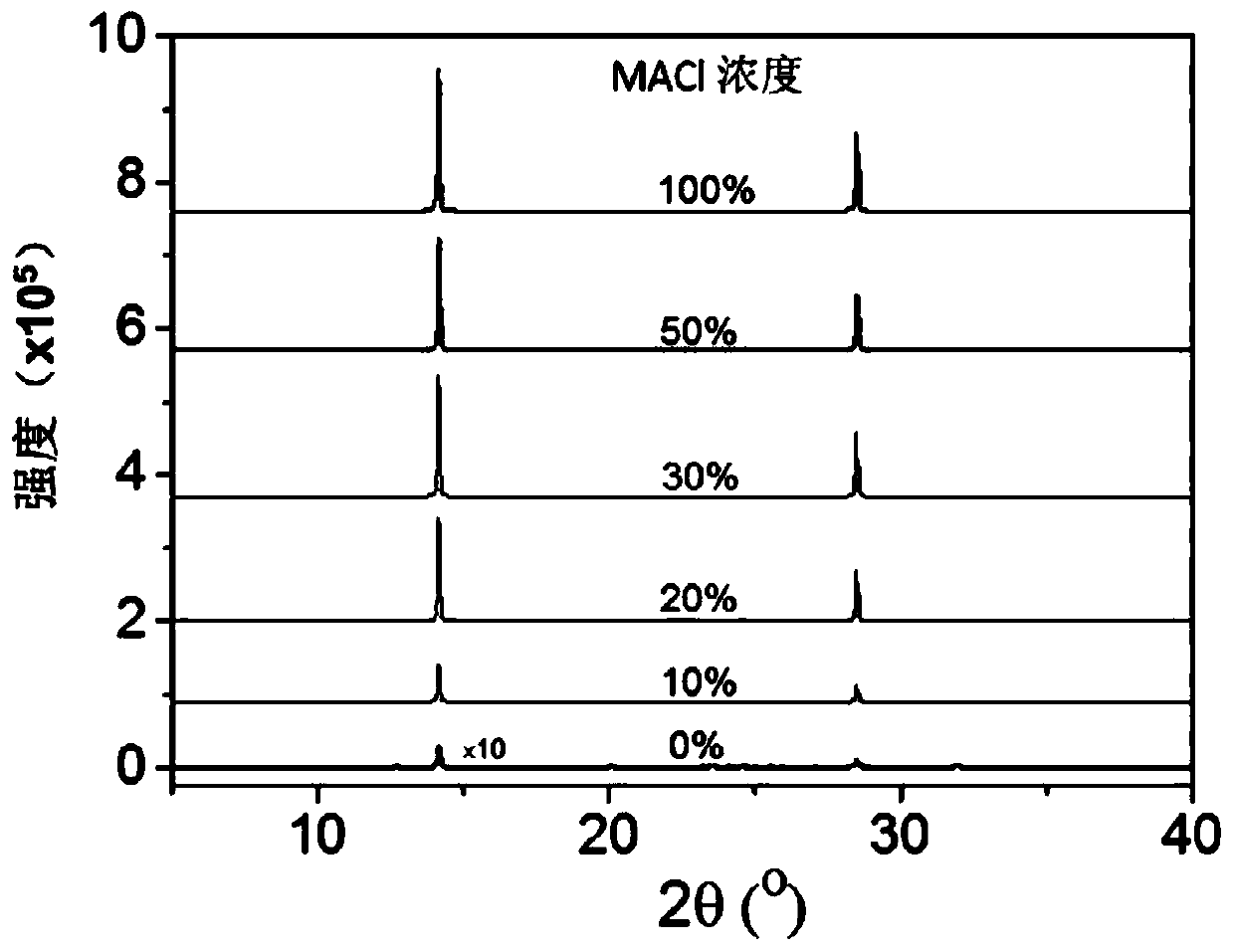
[0048] Embodiment 1 prepares the MAPbI that contains the MACl additive of different additions 3 film
[0049] (1) MAI and PbI 2 Soluble in a mixed organic solvent with a volume ratio of DMF:DMSO=4:1 (MAI=1M, PbI 2 =1M), and mixed uniformly to obtain a precursor solution. Then respectively add 0%, 10%, 20%, 30%, 50% and 100% of the MACl additive relative to the molar concentration of the precursor solution (1M), to obtain different concentrations of MACl (0M, 0.1M, 0.2M, 0.3M, 0.5M, 1M) mixed solution;
[0050] (2) In a glove box with a room temperature of 25°C, set the height difference between the scraper and the substrate to 200 μm, and apply the mixed solutions containing different concentrations of MACl obtained in step (1) with an amount of 20 μL, using a scraping speed of 8 mm / s. Distributed on the glass substrate to obtain a precursor wet film;
[0051] (3) Put the obtained precursor wet film into a vacuum chamber, pump air at a speed of 100 Pa / s at 25°C to make th...
Embodiment 2
[0054] Embodiment 2 prepares the FA containing the MACl additive of different additions 0.6 MA 0.4 Pb(I 0.6 Br 0.4 ) 3 Thin film (1) MABr, FAI, PbBr 2 and PbI 2 Soluble in DMF:DMSO=4:1 (v:v) mixed organic solvent (MABr=0.4M, FAI=0.6M, PbBr 2 =0.4M, PbI 2 =0.6M), obtain the precursor solution, then add respectively 0%, 10%, 20% and 30% of the MACl additive relative to the precursor solution molar concentration (1M), to obtain different concentrations of MACl (0M, 0.1M, 0.2M, 0.3M) mixed solution;
[0055] Step (2) and (3) are identical with embodiment 1 step (2) and (3);
[0056] (4) The obtained mesophase perovskite film was annealed at 120°C on a heating platform for 10 minutes to obtain FA with different shapes. 0.6 MA 0.4 Pb(I 0.6 Br 0.4 ) 3 perovskite thin film.
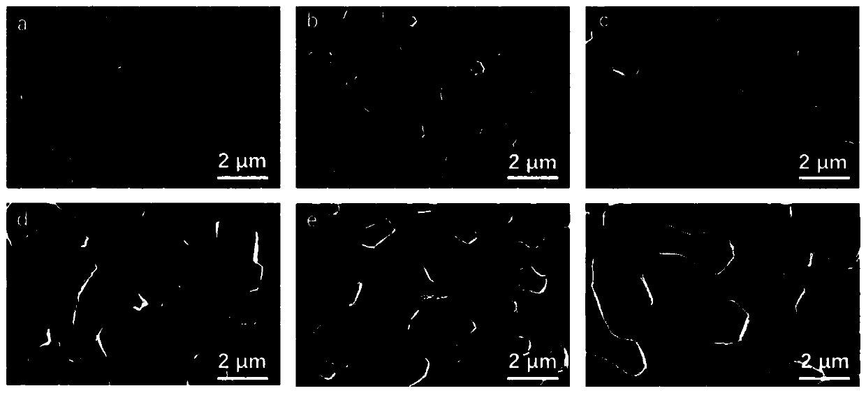
[0057] Figure 4 FA was prepared for Example 2 0.6 MA 0.4 Pb(I 0.6 Br 0.4 ) 3 The magnification of the film is 10000 times the SEM image, where Figure a is 0% added amount of MACl, Figure b is...
Embodiment 3
[0058] Embodiment 3 prepares Sn-Pb mixed narrow bandgap (FASnI 3 ) 0.5 (MAPbI 3 ) 0.5 Perovskite polycrystalline film
[0059] (1) SnI 2 , SnF 2 and FAI are dissolved in DMF:DMSO=4:1 (v:v) mixed organic solvent (SnI 2 =1.0M, SnF 2 =1.0M, FAI=1.0M), FASnI was prepared 3 solution. MAI and PbI 2 Soluble in DMF: DMSO=9:1 (v:v) mixed organic solvent (wherein MAI=1.0M, PbI 2 =1.0M), the prepared MAPbI 3 solution, and then FASnI 3 solution and MAPbI 3 The solutions were mixed at a volume ratio of 1:1 to obtain a Pb-Sn mixed precursor solution (FASnI 3 ) 0.5 (MAPbI 3 ) 0.5 , then add 3% Pb(SCN) relative to the molar concentration (1.0M) of the precursor solution 2 Additive, made with 0.03M Pb(SCN) 2 The Sn-Pb mixed solution;
[0060] Step (2) and (3) are identical with embodiment 1 step (2) and (3);
[0061] (4) The obtained mesophase perovskite film was annealed at 100° C. on a heating platform for 10 minutes to obtain a Sn—Pb mixed perovskite film.
[0062] Fi...
PUM
| Property | Measurement | Unit |
|---|---|---|
| thickness | aaaaa | aaaaa |
| thickness | aaaaa | aaaaa |
| energy conversion efficiency | aaaaa | aaaaa |
Abstract
Description
Claims
Application Information


