LED chip and manufacturing method thereof, display panel and electronic device

A technology of LED chip and manufacturing method, which is applied in the direction of circuits, electrical components, electric solid devices, etc., can solve the problems of affecting the yield rate of display panels and increasing the number of dead pixels of Micro-LED display panels, so as to improve the yield rate and reduce the number of bad spots. The probability of point generation, the effect of increasing the contact area

Active Publication Date: 2021-08-17
CHENGDU VISTAR OPTEOLECTRONICS CO LTD
View PDF0 Cites 0 Cited by
  • Summary
  • Abstract
  • Description
  • Claims
  • Application Information

AI Technical Summary

Problems solved by technology

[0005] However, with the reduction of the electrode size of the LED chip, the number of dead pixels of the Micro-LED display panel increases exponentially, which affects the yield rate of the display panel

Method used


Image

  • LED chip and manufacturing method thereof, display panel and electronic device
  • LED chip and manufacturing method thereof, display panel and electronic device
  • LED chip and manufacturing method thereof, display panel and electronic device

Examples


Embodiment Construction

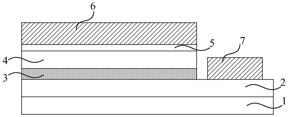
[0051] BACKGROUND OF THE INVENTION As the LED chip electrode size is reduced, the number of bad points in the Micro-LED display panel is multiplied, which affects the yield of the Micro-LED display panel. Now combined figure 1 Analyze the number of bad points in Micro-LED display panel:

[0052] During the manufacturing process of the actual micro-LED, in manufacturing figure 1 After the LED chip shown, the sapphire substrate 1 of the LED chip is removed, and a plurality of LED chips are powered on the drive backplane, thereby implementing the batch transfer of the LED chip.

[0053] Specifically, the bonding process is connected to the drive back plate by the welding process, thereby enabling the circuit unit on the drive back plate to the first contact electrode. 6 and the second contact electrode 7 loading voltage.

[0054] However, as the size of the LED chip is reduced, the size of the first contact electrode 6 and the second contact electrode 7 is reduced to several microns ...


PUM

PropertyMeasurementUnit
sizeaaaaaaaaaa
sizeaaaaaaaaaa
thicknessaaaaaaaaaa

Abstract

The invention provides an LED chip, a manufacturing method thereof, a display panel and electronic equipment. The manufacturing method includes: providing a substrate; sequentially forming a first semiconductor layer, an active layer, and a second semiconductor layer on the substrate; forming a electrically connecting the first contact electrode; forming a second contact electrode electrically connected to the second semiconductor layer on the second semiconductor layer; forming a second contact electrode electrically connected to the first contact electrode on the first contact electrode The first extended electrode, the first extended electrode includes a plurality of concave points for welding; forming on the second contact electrode electrically connected to the second contact electrode and isolated from the first extended electrode A second extended electrode including a plurality of dimples for welding. The invention improves the yield rate of the display panel.

Description

Technical field [0001] The present invention relates to a display technique, and more particularly to an LED chip and a manufacturing method thereof, a display panel, and an electronic device. Background technique [0002] Micro-LED Display is a new generation of display technology, which realizes image display as sub-pixel as sub-pixels. Compared to Liquid Crystal Display, LCDs, the Micro-LED display panel can implement image display without the external light source, improve the lightweight degree of display panels. Further, compared with the organic light-emitting diode, OLED, which can also be sponsors, and there is a long life of the MICRO-LED display panel and thus become the hotspots of the industry. [0003] refer to figure 1 It is a cross-sectional view of a prior art with an LED chip. The LED chip includes: sapphire substrate 1, sequentially located N-type gallium nitride 2, quantum well layer 3, and p-type gallium nitride 4 on sapphire substrate, indium tin oxide layer...

Claims


Application Information

Patent Timeline
Patent Type & Authority Patents(China)
IPC IPC(8): H01L33/38H01L33/00G09F9/33
CPCH01L33/382H01L33/005G09F9/33H01L33/38H01L33/00H01L33/36H10K59/00
Inventor 韦冬邢汝博刘会敏杨小龙王建太
Owner CHENGDU VISTAR OPTEOLECTRONICS CO LTD
Why Eureka
Try Eureka