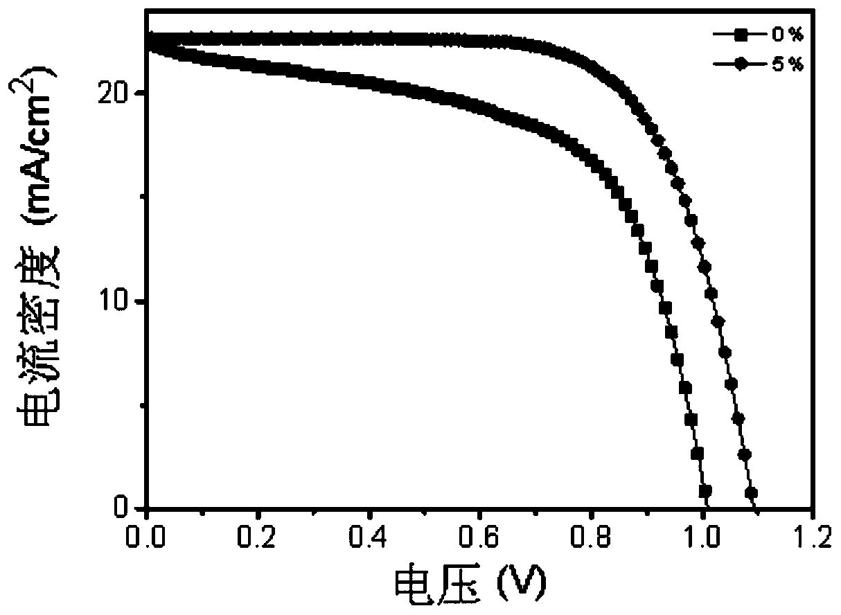
Perovskite solar cell with Bi2O2S modified SnO2 electron transfer layer and preparation method
An electron transport layer, solar cell technology, applied in semiconductor/solid-state device manufacturing, circuits, photovoltaic power generation, etc., can solve the problem of tin dioxide material deviating from the ideal stoichiometric ratio, etc., to reduce recombination, improve performance, and improve charge transfer. Effect
- Summary
- Abstract
- Description
- Claims
- Application Information
AI Technical Summary
Problems solved by technology
Method used
Image
Examples
Embodiment 1
[0030] A Bi of this embodiment 2 o 2 S-modified SnO 2 The perovskite solar cell device structure of the electron transport layer is: ITO / SnO 2 : Bi 2 o 2 S / MAPbI 3 / Spiro-OMeTAD / MoO x / Ag. The specific preparation process is as follows:
[0031] (1) The ITO substrate was ultrasonically cleaned with detergent, deionized water, acetone, absolute ethanol, and isopropanol in sequence for 20 minutes, and then dried in a vacuum oven at 80°C. The surface of the cleaned and dried ITO substrate is subjected to plasma surface treatment for 10 minutes. This treatment method utilizes the strong oxidizing properties of ozone generated under microwaves to clean the residual organic matter on the ITO surface, while improving the work function of the ITO surface.
[0032] (2) Spin-coat SnO on the ITO surface treated in step (1) 2 with Bi 2 o 2 S mixed solution, the rotation speed is 3500rpm, the time is 40s; followed by annealing treatment, the temperature is 180°C, the time is 1 h...
Embodiment 2
[0042] A Bi of this embodiment 2 o 2 S-modified SnO 2 The perovskite solar cell device structure of the electron transport layer is: ITO / SnO 2 : Bi 2 o 2 S / MAPbI 3 / Spiro-OMeTAD / MoO x / Ag. The specific preparation process is as follows:
[0043] (1) The ITO substrate was ultrasonically cleaned with detergent, deionized water, acetone, absolute ethanol, and isopropanol in sequence for 20 minutes, and then dried in a vacuum oven at 80°C. The surface of the cleaned and dried ITO substrate is subjected to plasma surface treatment for 10 minutes. This treatment method utilizes the strong oxidizing properties of ozone generated under microwaves to clean the residual organic matter on the ITO surface, while improving the work function of the ITO surface.
[0044] (2) Spin-coat SnO on the ITO surface treated in step (1) 2 with Bi 2 o 2 S mixed solution, the rotation speed is 3500rpm, the time is 50s; followed by annealing treatment, the temperature is 180°C, the time is 1 h...
Embodiment 3
[0048] A Bi of this embodiment 2 o 2 S-modified SnO 2 The perovskite solar cell device structure of the electron transport layer is: ITO / SnO 2 : Bi 2 o 2 S / MAPbI 3 / Spiro-OMeTAD / MoO x / Ag. The specific preparation process is as follows:
[0049] (1) The ITO substrate was ultrasonically cleaned with detergent, deionized water, acetone, absolute ethanol, and isopropanol in sequence for 20 minutes, and then dried in a vacuum oven at 80°C. The surface of the cleaned and dried ITO substrate is subjected to plasma surface treatment for 10 minutes. This treatment method utilizes the strong oxidizing properties of ozone generated under microwaves to clean the residual organic matter on the ITO surface, while improving the work function of the ITO surface.
[0050] (2) Spin-coat SnO on the ITO surface treated in step (1) 2 with Bi 2 o 2 S mixed solution, the rotation speed is 3500rpm, the time is 45s; followed by annealing treatment, the temperature is 180°C, the time is 1 h...
PUM
| Property | Measurement | Unit |
|---|---|---|
| Particle size | aaaaa | aaaaa |
| Thickness | aaaaa | aaaaa |
| Thickness | aaaaa | aaaaa |
Abstract
Description
Claims
Application Information
 - R&D
- Intellectual Property
- Life Sciences
- Materials
- Tech Scout
- Unparalleled Data Quality
- Higher Quality Content
- 60% Fewer Hallucinations
Browse by: Latest US Patents, China's latest patents, Technical Efficacy Thesaurus, Application Domain, Technology Topic, Popular Technical Reports.
© 2025 PatSnap. All rights reserved.Legal|Privacy policy|Modern Slavery Act Transparency Statement|Sitemap|About US| Contact US: help@patsnap.com


