Flexile inner-connected CIGS solar cell and preparation method thereof
A solar cell and flexible technology, applied in the field of solar cells, can solve the problems of small reduction in cell manufacturing cost, very high component efficiency loss, and complicated welding process, so as to improve component efficiency, suppress the generation of low-level defect states, and avoid dead The effect of a large area
- Summary
- Abstract
- Description
- Claims
- Application Information
AI Technical Summary
Problems solved by technology
Method used
Image
Examples
Embodiment 1
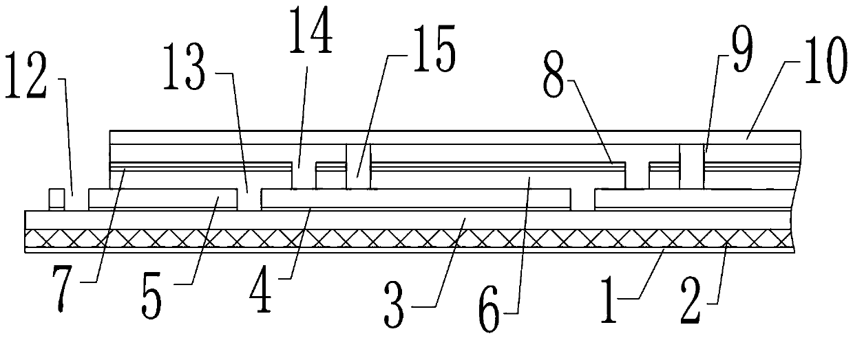
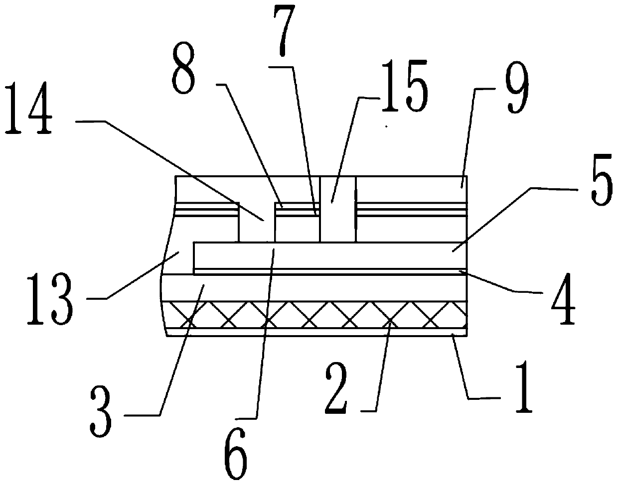
[0052] Step 1. Prepare a 1500nm thick aluminum nitride insulating layer on a flexible stainless steel substrate with a thickness of 30um. The preparation method is the reactive magnetron sputtering method. The sputtering target material used is aluminum, and the N 2 and Ar mixed gas, the background vacuum degree during sputtering is less than or equal to 5.0×10 ﹣3 Pa, the power density is 0.1W / cm 2 , working pressure is 0.1Pa, stainless steel substrate temperature is 20℃, sputtering time is 5min, N 2 The flow rate is 10-30sccm, and the Ar flow rate is 90sccm;
[0053] Step 2: Prepare a chromium barrier layer with a thickness of 100nm on the insulating layer by DC sputtering. The target material used in the preparation is a chromium target. Ar is introduced during the preparation process. The background vacuum degree during sputtering is less than or equal to 5.0× 10 ﹣3 Pa, sputtering power 3kW, working pressure 0.5Pa, stainless steel substrate temperature 20°C, sputtering ...
Embodiment 2
[0062] Step 1. Prepare an insulating layer with a thickness of 1800nm on a flexible stainless steel substrate with a thickness of 40um. The preparation method is the reactive magnetron sputtering method. The sputtering target material used is aluminum, and N is introduced during sputtering. 2 and Ar mixed gas, the background vacuum degree during sputtering is less than or equal to 5.0×10 ﹣3 Pa, the power density is 10W / cm 2 , working pressure is 8Pa, stainless steel substrate temperature is 100℃, sputtering time is 10min, N 2 The flow rate is 20sccm, and the Ar flow rate is 100sccm;
[0063] Step 2: Prepare a chromium barrier layer with a thickness of 100nm by DC sputtering on the aluminum nitride insulating layer. The target material used in the preparation is a chromium target. Ar is introduced during the preparation process. The background vacuum during sputtering is less than Equal to 5.0×10 ﹣3 Pa, sputtering power 5kW, working pressure 0.5-0.8Pa, stainless steel subs...
Embodiment 3
[0072]Step 1. Prepare a 2000nm thick aluminum nitride insulating layer on a flexible stainless steel substrate with a thickness of 50um. The preparation method is the reactive magnetron sputtering method. The sputtering target material used is aluminum, and the N 2 and Ar mixed gas, the background vacuum degree during sputtering is less than or equal to 5.0×10 ﹣3 Pa, the power density is 20W / cm 2 , the working pressure is 10Pa, the stainless steel substrate temperature is 400°C, the sputtering time is 20min, the N2 flow rate is 30sccm, and the Ar flow rate is 150sccm;
[0073] Step 2: Prepare a chromium barrier layer with a thickness of 100nm by DC sputtering on the aluminum nitride insulating layer. The target material used in the preparation is a chromium target. Ar is introduced during the preparation process. The background vacuum during sputtering is less than Equal to 5.0×10 ﹣3 Pa, sputtering power 6kW, working pressure 0.8Pa, stainless steel substrate temperature 400...
PUM
| Property | Measurement | Unit |
|---|---|---|
| Thickness | aaaaa | aaaaa |
| Thickness | aaaaa | aaaaa |
| Thickness | aaaaa | aaaaa |
Abstract
Description
Claims
Application Information


