
Optical colorful thin film and manufacturing method thereof

A production method and colorful technology, applied in the direction of ion implantation plating, metal material coating process, coating, etc., can solve the problems of difficult appearance decoration, poor wear resistance, etc., and achieve improved performance and high wear resistance. , good colorful and beautiful effect

Active Publication Date: 2019-10-25
SHENZHEN SENFUNG VACUUM PLATING
View PDF2 Cites 2 Cited by
  • Summary
  • Abstract
  • Description
  • Claims
  • Application Information

AI Technical Summary

Problems solved by technology

Due to the poor wear resistance of optical films prepared by traditional magnetron sputtering, it is difficult to use them on decorative parts

Method used


Image

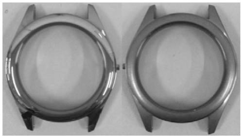
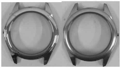
  • Optical colorful thin film and manufacturing method thereof
  • Optical colorful thin film and manufacturing method thereof

Examples


Embodiment 1

[0055] 1. Charge a certain amount of Ar to start the arc power supply in a high vacuum state for ion cleaning, remove the fine dust on the surface of the product and activate its surface to increase the binding force between the membrane bases.

[0056] 2. Fill in 110-130sccm working gas Ar and 70-90sccm reaction gas O2, maintain the air pressure at 0.3pa-0.4pa, first turn on the titanium target, target current at 22-27A, deposit TiO2 layer, deposition time 25-35 minutes to form the first layer.

[0057] 3. Fill in 110-130sccm working gas Ar and 70-90sccm reaction gas O2, maintain the air pressure at 0.3pa-0.4pa, open the silicon target, target current at 18-22A, deposit SiO2 layer, deposition time 7-13 minutes , forming the second layer.

[0058] 4. Deposit the third and fifth layers with reference to the process parameters of the first layer, and deposit the fourth and sixth layers with reference to the process parameters of the second layer.

[0059] 5. Fill in 110-130scc...

Embodiment 2

[0061] 1. Charge a certain amount of Ar to start the arc power supply in a high vacuum state for ion cleaning, remove the fine dust on the surface of the product and activate its surface to increase the binding force between the membrane bases.

[0062] 2. Then fill in 120sccm of Ar and 80sccm of O2, the air pressure is 0.3pa-0.4pa, first open the titanium target to form a layer of dense TiO2 deposited on the product, the time is 27 minutes, and the first layer is formed at this time.

[0063] 3. Fill 120sccm of Ar and 80sccm of O2, turn on the silicon target to form a layer of dense SiO2 deposited on the product for 7 minutes, and form the second layer at this time.

[0064] 4. Deposit the third and fifth layers with reference to the process parameters of the first layer, and deposit the fourth and sixth layers with reference to the process parameters of the second layer.

[0065] 5. Fill in 110-130sccm working gas Ar and 70-90sccm reaction gas O2, maintain the air pressure a...

Embodiment 3

[0067] 1. Charge a certain amount of Ar to start the arc power supply in a high vacuum state for ion cleaning, remove the fine dust on the surface of the product and activate its surface to increase the binding force between the membrane bases.

[0068] 2. Then fill in 120sccm of Ar and 80sccm of O2, the air pressure is 0.3pa-0.4pa, first open the titanium target to form a layer of dense TiO2 deposited on the product, the time is 32 minutes, and the first layer is formed at this time.

[0069] 3. Fill in 120 sccm of Ar and 80 sccm of O2, turn on the silicon target to form a layer of dense SiO2 deposited on the product for 11 minutes, and form the second layer at this time.

[0070] 4. Deposit the third and fifth layers with reference to the process parameters of the first layer, and deposit the fourth and sixth layers with reference to the process parameters of the second layer.

[0071] 5. Fill in 110-130sccm working gas Ar and 70-90sccm reaction gas O2, maintain the air pres...


PUM


Abstract

The invention provides an optical colorful thin film and a manufacturing method. The method includes the steps that S1, a TiO2 layer is deposited on the surface of a substrate material to serve as a first layer; S2, a SiO2 layer is deposited on the first layer to serve as a second layer; S3, a TiO2 layer is deposited on the second layer to serve as a third layer; S4, a SiO2 layer is deposited on the third layer to serve as a fourth layer; S5, a TiO2 layer is deposited on the fourth layer to serve as a fifth layer; S6, a SiO2 layer is deposited on the fifth layer to serve as a sixth layer; andS7, a TiO2 layer is deposited on the sixth layer to serve as a seventh layer. The deposition process of the multi-layer film is controlled, the multi-layer film is colorful, and the seventh layer, namely the outermost layer continues to be deposited for 40-50 minutes under the state that the multi-layer film is kept colorful. According to the optical colorful thin film and the manufacturing method, the anti-abrasion performance of the optical thin film is greatly improved, and meanwhile the colorful effect of the optical thin film is guaranteed.

Description

technical field [0001] The invention relates to the field of optical films, in particular to an optical colorful film and a manufacturing method thereof. Background technique [0002] The preparation technology of optical thin films is to deposit thin film materials into thin films according to certain technical approaches and specific requirements. With the development of modern information optics, optoelectronic technology and photon technology, the requirements for long life, high reliability and high strength of optical thin films are getting higher and higher, thus a series of new optical thin films and their preparation technologies have been developed. These technologies are used in the preparation of optical thin films, which not only greatly broadens the range of materials available for optical thin films, but also greatly improves the performance and functions of optical thin films. Optical thin films can be prepared by physical vapor deposition (PVD), chemical va...

Claims


Application Information

Patent Timeline
IPC IPC(8): C23C14/35C23C14/08C23C14/10
CPCC23C14/0015C23C14/0036C23C14/083C23C14/10C23C14/352
Inventor 赵明华吴吉诚武俊伟汪选林
Owner SHENZHEN SENFUNG VACUUM PLATING
Learn More