A method for manufacturing a multi-layer PCB board with a groove-type buried copper block

A technology of PCB board and production method, which is applied in the direction of multilayer circuit manufacturing, printed circuit manufacturing, and improvement of metal adhesion of insulating substrates, and can solve problems such as easy tin climbing.

Active Publication Date: 2021-07-06
WUS PRINTED CIRCUIT (KUNSHAN) CO LTD
View PDF11 Cites 0 Cited by
  • Summary
  • Abstract
  • Description
  • Claims
  • Application Information

AI Technical Summary

Problems solved by technology

[0007] In view of the above problems, the present invention proposes a multi-layer PCB board with recessed buried copper blocks and its manufacturing method, which can avoid the quality risk of tin creeping in the traditional method of assembly, and solve the problem of the traditional method of mandatory pattern electroplating. troubles and limitations

Method used


Image

  • A method for manufacturing a multi-layer PCB board with a groove-type buried copper block
  • A method for manufacturing a multi-layer PCB board with a groove-type buried copper block
  • A method for manufacturing a multi-layer PCB board with a groove-type buried copper block

Examples


Embodiment Construction

[0036] In order to make the objectives, technical solutions and advantages of the present invention, the present invention will be further described in detail below with reference to the embodiments. It will be appreciated that the specific embodiments described herein are intended to be used to explain the invention and are not intended to limit the scope of the invention.

[0037] The application principles of the present invention will be described in detail below with reference to the drawings.

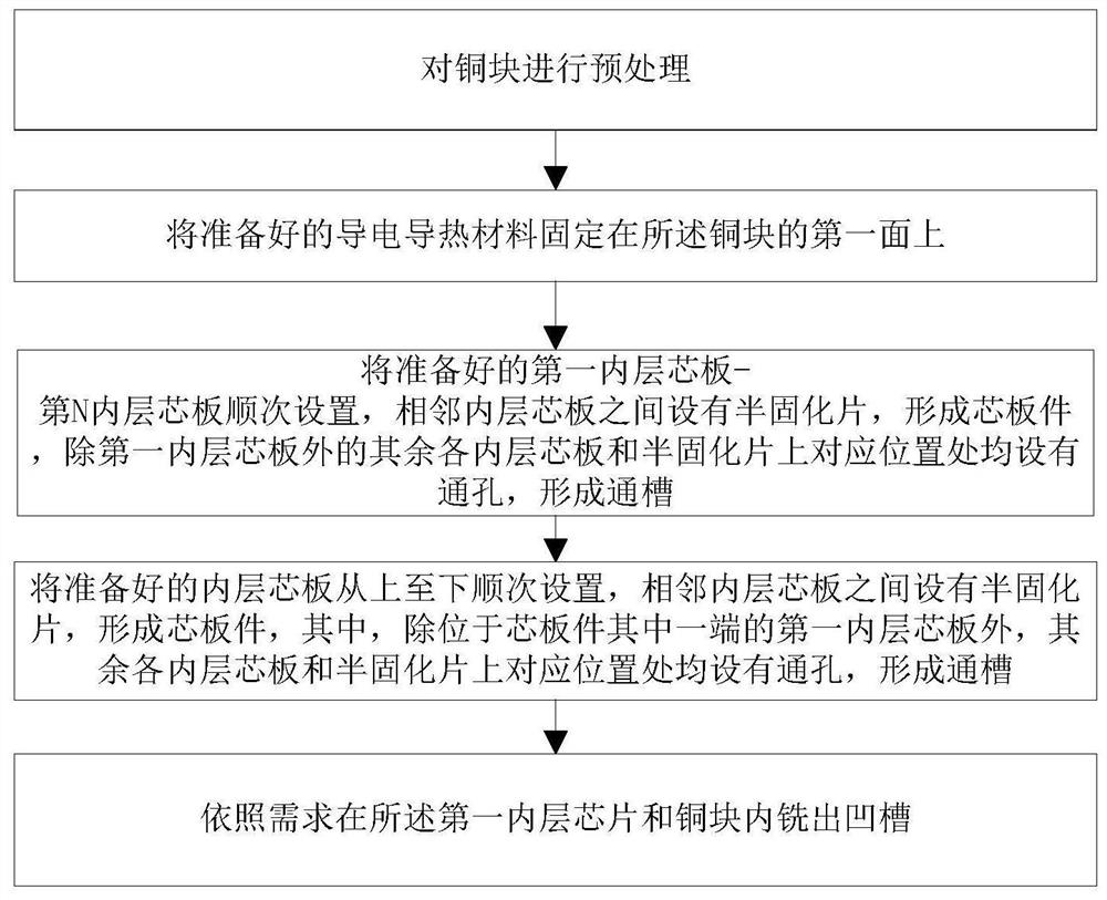
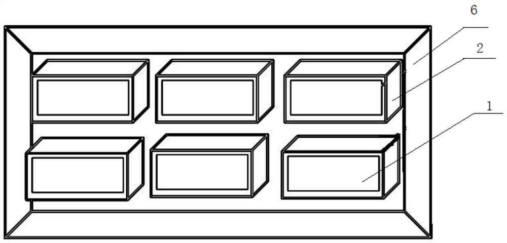
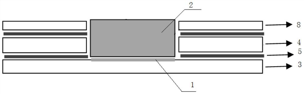
[0038] Such as figure 1 As shown, the present invention provides a multilayer PCB plate fabrication method for groove type buried copper blocks, including the following steps:

[0039] (1) Pretreatment of copper block 2;

[0040] In a specific embodiment of an embodiment of the present invention, the step (1) is specifically:

[0041] Copper block 2 is carried out;

[0042] In another embodiment of the embodiment of the invention, the step (1) is specifically:

[0043] Black treatment...


PUM


Abstract

The invention discloses a method for manufacturing a multi-layer PCB board with groove-type embedded copper blocks, which includes pretreating the copper blocks; fixing the prepared conductive and heat-conducting materials on the first surface of the copper blocks; One inner layer core board...Nth inner layer chips are arranged in sequence, and prepregs are arranged between adjacent inner layer core boards to form core board parts, and the other inner layer core boards and prepregs except the first inner layer core board Through holes are provided at the corresponding positions on the top to form a through groove; the copper block is put into the through groove so that the conductive and heat-conducting material is located between the first surface of the copper block and the first inner core board, and pressed together; according to Recesses need to be milled in the first inner chip and copper block. By using special conductive and heat-conducting materials and a unique operation method, the present invention relatively easily realizes the design purpose of the groove of the traditional power amplifier, avoids the quality risk of tin climbing in the traditional method of assembly, and solves the traditional method of mandatory graphics Problems and limitations of electroplating.

Description

Technical field [0001] The present invention belongs to the technical field of PCB plate making, and more particularly to a multilayer PCB plate fabrication method for groove type buried copper blocks. Background technique [0002] At present, the production of a multilayer amplifier printed circuit board for groove type buried copper block is widely used to complete the processing of PCB and combined with graphic electroplating, so that the copper block, the core plate and the semi-solidified sheet are pressed, first controlled The copper block groove is deep milling. After the electroplating is completed, the side wall copper with a deep milling of the deep milling mill is used, so that the power amplifier high-speed pattern and ground layer are broken, and reduce the amplifier welding Tin ultrasound short-circuit risk. The disadvantages of this method include: [0003] 1) The copper block and the RF double panel above it are large copper surfaces, which use traditional FR4 mat...

Claims


Application Information

Patent Timeline
Patent Type & Authority Patents(China)
IPC IPC(8): H05K1/18H05K3/46H05K1/02H05K3/38
CPCH05K1/0204H05K1/183H05K3/382H05K3/4697
Inventor 张涛周军
Owner WUS PRINTED CIRCUIT (KUNSHAN) CO LTD
Why Eureka
Try Eureka