Carbon-based film for inhibiting secondary electron emission and preparation method thereof

A secondary electron emission, carbon-based technology, used in sputtering, ion implantation, vacuum evaporation, etc., can solve the problems of complex application environment, improve surface roughness, reduce secondary electrons Ejection chance, the effect of increasing the content

Pending Publication Date: 2019-11-01
XI AN JIAOTONG UNIV
View PDF6 Cites 6 Cited by
  • Summary
  • Abstract
  • Description
  • Claims
  • Application Information

AI Technical Summary

Problems solved by technology

However, with the continuous improvement of practical application requirements, the power of microwave devices and particle accelerators and other devices is also increasing, and the application environment is more complex. It is necessary to further improve the ability of amorphous carbon films to suppress the secondary electron emission of metals and insulator materials. In order to reduce the adverse effects of micro-discharge and electron cloud equivalent on the device

Method used


Image

  • Carbon-based film for inhibiting secondary electron emission and preparation method thereof
  • Carbon-based film for inhibiting secondary electron emission and preparation method thereof
  • Carbon-based film for inhibiting secondary electron emission and preparation method thereof

Examples


Embodiment 1

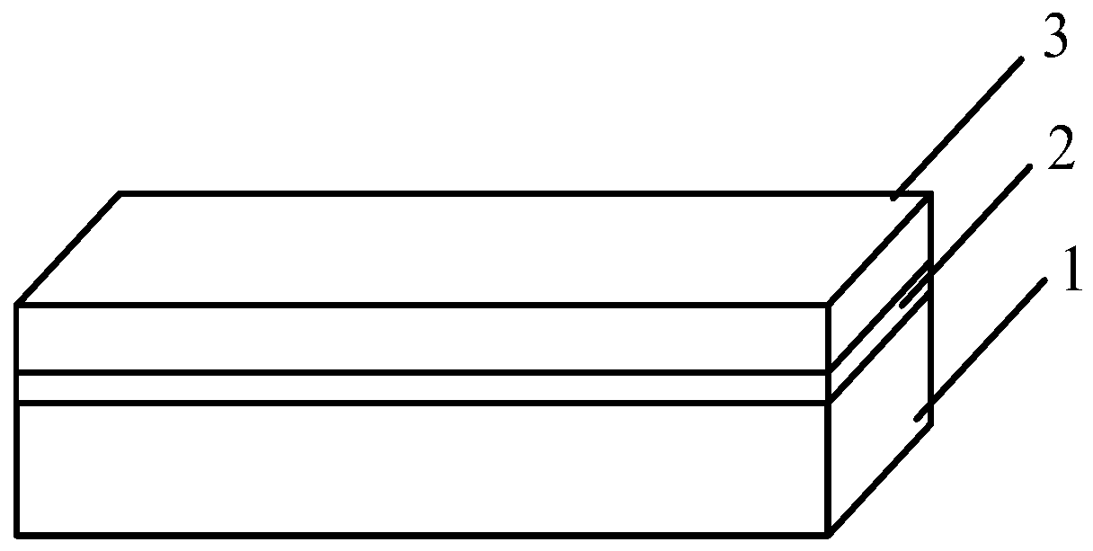
[0023] see figure 1 The carbon-based thin film of the present invention is composed of a titanium buffer layer 2 and an amorphous carbon film layer 3 sequentially arranged on the surface of a substrate 1 from bottom to top. The preparation method specifically includes the following steps:

[0024] 1) The titanium buffer layer 2 is deposited on the substrate 1 by direct current sputtering titanium target method. During the deposition process, the substrate temperature is kept at 400°C, argon gas is introduced into the coating chamber, and the pressure in the coating chamber is 0.1Pa. The thickness of the titanium buffer layer 2 is 12 nm.

[0025] 2) The amorphous carbon film layer 3 is deposited on the titanium buffer layer 2 by using the radio frequency sputtering graphite target method. During the deposition process, the substrate temperature is maintained at 350°C, argon gas is introduced into the coating chamber, and the pressure in the coating chamber is 0.2Pa, the thick...

Embodiment 2

[0027] see figure 1 The carbon-based thin film of the present invention is composed of a titanium buffer layer 2 and an amorphous carbon film layer 3 sequentially arranged on the surface of a substrate 1 from bottom to top. The preparation method specifically includes the following steps:

[0028] 1) The titanium buffer layer 2 is deposited on the substrate 1 by direct current sputtering titanium target. During the deposition process, the substrate temperature is kept at 450°C, argon gas is introduced into the coating chamber, and the pressure in the coating chamber is 0.3Pa. The thickness of the titanium buffer layer 2 is 20 nm.

[0029] 2) The amorphous carbon film layer 3 is deposited on the titanium buffer layer 2 by using the radio frequency sputtering graphite target method. During the deposition process, the substrate temperature is kept at 420°C, argon gas is introduced into the coating chamber, and the pressure in the coating chamber is 0.9Pa, the thickness of the d...

Embodiment 3

[0032] see figure 1 The carbon-based thin film of the present invention is composed of a titanium buffer layer 2 and an amorphous carbon film layer 3 sequentially arranged on the surface of a substrate 1 from bottom to top. The preparation method specifically includes the following steps:

[0033] 1) The titanium buffer layer 2 is deposited on the substrate 1 by direct current sputtering titanium target method. During the deposition process, the substrate temperature is maintained at 500°C, argon gas is introduced into the coating chamber, and the pressure in the coating chamber is 0.5Pa. The thickness of the titanium buffer layer 2 is 30 nm.

[0034]2) The amorphous carbon film layer 3 is deposited on the titanium buffer layer 2 by using the radio frequency sputtering graphite target method. During the deposition process, the substrate temperature is kept at 500°C, argon gas is introduced into the coating chamber, and the pressure in the coating chamber is 0.3Pa, the thickn...


PUM

PropertyMeasurementUnit
thicknessaaaaaaaaaa
thicknessaaaaaaaaaa
sizeaaaaaaaaaa

Abstract

The invention discloses a carbon-based film for inhibiting secondary electron emission and a preparation method thereof. The film is composed of a metal buffer layer and an amorphous carbon film layer, wherein the thickness of the metal buffer layer is 5-50 nm, the thickness of the amorphous carbon film layer is 30-200 nm, the size of carbon particles in the amorphous carbon film layer is 20-100 nm, and metal materials in the metal buffer layer is titanium, molybdenum or tungsten. The preparation method of the carbon-based film comprises the following steps that firstly, the metal buffer layeris deposited on a base in a metal target sputtering mode under the condition that the temperature of the base is 400-600 DGE C; then, the amorphous carbon film layer is deposited on the metal bufferlayer in a graphite target sputtering mode under the condition that the temperature of the base is 300-600 DGE C; and finally, the amorphous carbon film layer is subjected to high-temperature annealing treatment or/and sputtering treatment is carried out on the surface of the amorphous carbon film layer by argon ions. According to the carbon-based film prepared by the method, the content of sp2 bonds and the surface roughness of an amorphous carbon film can be improved, so that the secondary electron emission coefficient of the amorphous carbon film is reduced.

Description

technical field [0001] The invention relates to the technical fields of microwave devices, particle accelerators, etc., in particular to a carbon-based thin film for suppressing secondary electron emission and a preparation method thereof. Background technique [0002] When particles such as electrons and ions with a certain energy or speed bombard solid materials such as metals, semiconductors, and insulators, the electrons inside the material will be excited and emitted from the surface. This physical phenomenon is called secondary electron emission. The secondary electron emission phenomenon can be used to double the number of electrons to achieve the amplification of weak photoelectric signals. Therefore, secondary electron emission is widely used in low-light imaging, atomic frequency standards, satellite navigation, mass spectrometry and energy spectrum analysis, microanalysis, and medical treatment. It has important applications in many technical fields such as inspec...

Claims


Application Information

Patent Timeline
Patent Type & Authority Applications(China)
IPC IPC(8): C23C14/34C23C14/16C23C14/06C23C14/58C23C14/02
CPCC23C14/025C23C14/0605C23C14/165C23C14/34C23C14/5806C23C14/5833
Inventor 胡文波易兴康李洁高步宇李永东吴胜利林舒
Owner XI AN JIAOTONG UNIV
Why Eureka
Try Eureka