Planar gate device structure having high switching speed and manufacturing method thereof

A technology of switching speed and device structure, used in semiconductor devices, electrical components, circuits, etc.

Pending Publication Date: 2019-11-08
ANHUI PROVINCE QIMEN COUNTY HUANGSHAN ELECTRIC APPLIANCE
View PDF0 Cites 0 Cited by
  • Summary
  • Abstract
  • Description
  • Claims
  • Application Information

AI Technical Summary

Problems solved by technology

[0003] One of the purposes of the present invention is to provide a planar gate device structure with high switching speed, which solves the

Method used


Image

  • Planar gate device structure having high switching speed and manufacturing method thereof
  • Planar gate device structure having high switching speed and manufacturing method thereof
  • Planar gate device structure having high switching speed and manufacturing method thereof

Examples


Embodiment 1

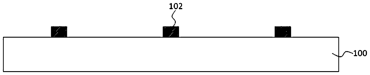
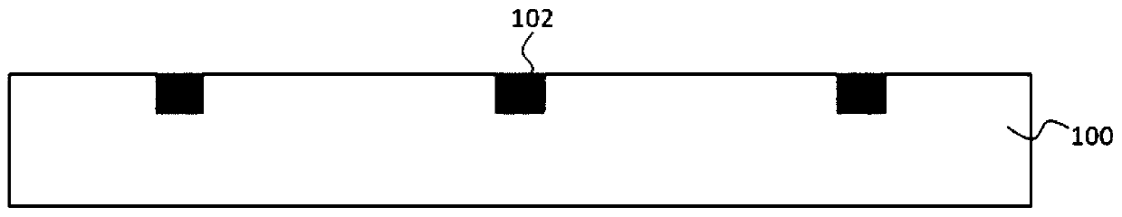
[0044] A planar gate device structure with high switching speed, such as Figure 7a As shown, a semiconductor substrate or epitaxial layer 100 is included, and a group of planar gates 10 are arranged on the surface of the semiconductor substrate or epitaxial layer 100 . The planar gate 10 includes a first gate electrode insulating layer 102 arranged in the middle, and the first gate electrode insulating layer 102 extends upward from the surface of the semiconductor substrate or the epitaxial layer 100 to protrude from the semiconductor substrate or the epitaxial layer 100 s surface. The second gate electrode insulating layer 103 extending from the first gate electrode insulating layer 102 to both sides and the gate electrode 104 arranged on the first gate electrode insulating layer 102 and the second gate electrode insulating layer 103, the first gate electrode The thickness of the insulating layer 102 is greater than that of the second gate electrode insulating layer 103 . ...

Embodiment 2

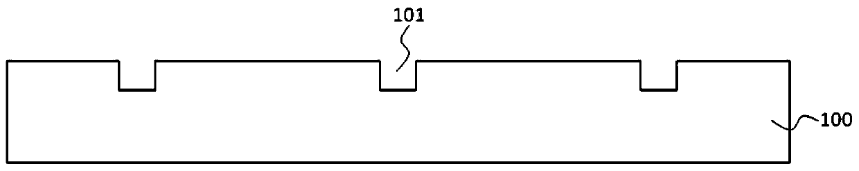
[0062] A planar gate device structure with high switching speed, such as Figure 7b As shown, it includes a semiconductor substrate or an epitaxial layer 100, and a group of planar gates 10 are arranged on the surface of the semiconductor substrate or epitaxial layer 100, and the planar gate 10 includes a first gate electrode insulating layer 102 arranged in the middle, so The first gate electrode insulating layer 102 extends downward from the surface of the semiconductor substrate or the epitaxial layer 100 and sinks into the semiconductor substrate or the epitaxial layer 100 . And the distance between the first gate insulating layer 102 and the first doped region 105 is greater than the carrier diffusion length between the first gate insulating layer 102 and the first doped region 105 when the device is turned on. The second gate electrode insulating layer 103 extending from the first gate electrode insulating layer 102 to both sides and the gate electrode 104 arranged on th...


PUM

PropertyMeasurementUnit
Thicknessaaaaaaaaaa
Thicknessaaaaaaaaaa
Thicknessaaaaaaaaaa

Abstract

The invention discloses a planar gate device structure having a high switching speed and a manufacturing method thereof. The planar gate device structure comprises a semiconductor substrate or an epitaxial layer, and a set of planar gates are arranged on the semiconductor substrate or the epitaxial layer, each planar gate comprises a first gate electrode insulation layer arranged at the middle position, a second gate electrode insulation layer extended from the first gate electrode insulation layer to the two sides, and a gate electrode arranged on the first gate electrode insulation layer andthe second gate electrode insulation layer, wherein the thickness of the first gate electrode insulation layer is larger than the thickness of the second gate electrode insulation layer. The manufacturing method of the planar gate is simple and easy to achieve, the device having the planar gate structure has lower gate and drain capacitance, the faster switching speed and the lower switching loss, and can be widely applied to the power semiconductor device fields such as MOSFET, IGBT and MCT.

Description

technical field [0001] The invention relates to the field of power semiconductor devices, in particular to a planar gate device structure with high switching speed and a manufacturing method thereof. Background technique [0002] The planar gate structure is often used in high withstand voltage power semiconductor devices, especially in power semiconductor devices with MOS structures such as MOSFETs, IGBTs, and MCTs. Compared with devices with traditional bipolar structure, devices with MOS structure are known for their high switching speed, and are mainly used in high-speed switching circuits. The large or small parasitic capacitance of the device directly affects the slow or fast switching speed of the device, and also affects the high or low switching power consumption of the device. In a common planar gate structure power semiconductor device, there is only one gate electrode insulating layer under the gate electrode, which corresponds to the second gate electrode insul...

Claims


Application Information

Patent Timeline
IPC IPC(8): H01L29/423H01L29/06
CPCH01L29/0603H01L29/0684H01L29/42356H01L29/42364
Inventor 饶祖刚王民安项建辉郑科峰
Owner ANHUI PROVINCE QIMEN COUNTY HUANGSHAN ELECTRIC APPLIANCE
Why Eureka
Try Eureka