Miniaturized high-density system-level logic circuit

A logic circuit, high-density technology, applied in logic circuits, logic circuits using specific components, logic circuits using basic logic circuit components, etc. The PAD arrangement is simple and reasonable, the number of PADs is reduced, and the circuit volume is reduced.

Active Publication Date: 2019-11-12
CETC GUOJI SOUTHERN GRP CO LTD
View PDF6 Cites 0 Cited by
  • Summary
  • Abstract
  • Description
  • Claims
  • Application Information

AI Technical Summary

Problems solved by technology

[0012] In traditional FPGA devices, all functional PADs are fan-out, the number of PADs is large, the arrangement is complex, and the device is large in size; when the FPGA is working, a reference clock must be provided externally as the working clock, and the reference clock will interfere with the radio frequency circuit. It may even cause the circuit to fail to work normally; FPGA storage data is usually connected to an external dedicated storage device, which is large in size and complex in circuit; when designing the PCB of the FPGA system, at least 10 layers of layout are required, and the design of PCB layout is difficult and the processing cycle is long. product development cycle

Method used


Image

  • Miniaturized high-density system-level logic circuit
  • Miniaturized high-density system-level logic circuit
  • Miniaturized high-density system-level logic circuit

Examples


Embodiment

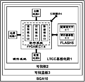
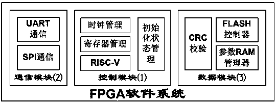
[0107] combine Figure 2~Figure 4 , the logic circuit hardware system provided by the present invention is composed of 10 parts, including LTCC substrate circuit 1, Kovar frame 2, Kovar cover plate 3, FPGA bare chip 4, FLASH bare chip 5, wire bonding 6, power supply circuit 7, Configuration circuit 8, decoupling circuit 9 and BGA10.

[0108] Such as Figure 5 As shown, the logic circuit of the present invention adopts a chip stacking structure, and the FPGA bare chip 4 and the FLASH bare chip 5 are assembled on the TOP layer of the circuit through pyramidal stacking.

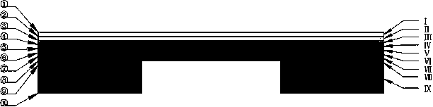
[0109] Such as Image 6 As shown, the logic circuit of the present invention adopts a wire bonding structure, including FPGA bare chip outer layer PAD4-1, FPGA bare chip inner layer PAD4-2, FLASH bare chip PAD5-1, ceramic base outer layer bonding PAD1-1 , Ceramic base middle layer bonding PAD1-2, ceramic base inner layer bonding PAD1-3, outer layer wire bonding 6-1, middle layer wire bonding 6-2, inner layer ...


PUM


Abstract

The invention relates to a miniaturized high-density system-level logic circuit. FPGA minimum system circuits such as an FPGA bare chip, a FLASH bare chip, a power supply circuit, a decoupling circuitand a configuration circuit are realized in a miniaturized ceramic circuit; on hardware, through ten-layer high-density ceramic circuit wiring, pyramid chip stacking and a ceramic cavity opening process, three-dimensional integration miniaturization of the circuit is achieved, an oscillator calibration circuit is achieved in an FPGA, and a dynamic oscillator frequency calibration function is achieved through a negative feedback loop. Hardware potential is fully excavated, innovation is achieved from a software architecture, the parallel computing capacity of an FPGA and the storage characteristic of FLASH are brought into play, a logic control circuit, a communication circuit and a data management circuit are customized and designed, and a powerful and complex logic function and a memoryfunction are achieved in combination with an RISC-V controller; the logic circuit has the advantages of high integration level, small size, high reliability, programmability, memorability and the like.

Description

technical field [0001] The invention is a miniaturized high-density system-level logic circuit, which belongs to the technical field of system circuits. Background technique [0002] Since the 1990s, portable, miniaturized electronic products, aerospace, and military electronics have entered a period of rapid development, requiring semiconductor devices to maximize miniaturization, light weight, and high density while meeting high reliability. Integrated circuit technology came into being. However, the current process technology of integrated circuits has approached its physical limit, and Moore's Law will not be maintained. In this context, System in Package (SIP) is proposed as an important technology of "More than Moore". The concept of "Moore's Law" focuses on the level of system integration and provides a new direction for the development of the electronics industry. [0003] International Technology Roadmap for Semiconductors (ITRS, International Technology Roadmap ...

Claims


Application Information

Patent Timeline
IPC IPC(8): G06F15/78H03K19/177
CPCG06F15/7807H03K19/1774Y02D10/00
Inventor 杨进张君直
Owner CETC GUOJI SOUTHERN GRP CO LTD
Why Eureka
Try Eureka