Epitaxial structure of power semiconductor device and its preparation method

A power semiconductor and epitaxial structure technology, which is applied in semiconductor devices, semiconductor/solid-state device manufacturing, electrical components, etc., can solve problems such as inconsistent growth rates, affecting GaN crystal growth, and reducing the crystal quality of GaN layers, so as to reduce the formation of defects , improve the crystal quality and ensure the effect of performance

Active Publication Date: 2022-05-20
HC SEMITEK SUZHOU
View PDF2 Cites 0 Cited by
  • Summary
  • Abstract
  • Description
  • Claims
  • Application Information

AI Technical Summary

Problems solved by technology

-OH suspension bonds and -O suspension bonds will affect the growth of GaN crystals, resulting in inconsistent growth rates of GaN crystals in different regions of the AlN layer, forming defects in the GaN layer, reducing the crystal quality of the GaN layer, resulting in the inability to obtain high-quality GaN layer, which seriously affects the performance of power semiconductor devices

Method used


Image

  • Epitaxial structure of power semiconductor device and its preparation method
  • Epitaxial structure of power semiconductor device and its preparation method
  • Epitaxial structure of power semiconductor device and its preparation method

Examples


Embodiment Construction

[0034] In order to make the object, technical solution and advantages of the present invention clearer, the implementation manner of the present invention will be further described in detail below in conjunction with the accompanying drawings.

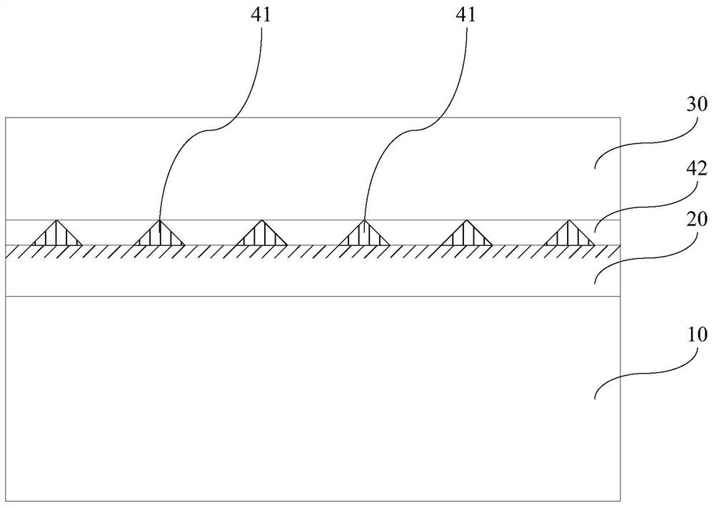
[0035] An embodiment of the present invention provides an epitaxial structure of a power semiconductor device. figure 1 A schematic structural diagram of an epitaxial structure of a power semiconductor device provided by an embodiment of the present invention. see figure 1 , the epitaxial structure of the power semiconductor device includes a Si substrate 10, an AlN buffer layer 20 and a GaN epitaxial layer 30 stacked in sequence, and the floating bonds on the first surface of the AlN buffer layer 20 include Al bonds, Ga bonds and N bonds. One or more, the first surface is the surface of the GaN epitaxial layer 30 disposed on the AlN buffer layer 20 .

[0036] In the embodiment of the present invention, by changing the AlN buffer lay...


PUM


Abstract

The invention discloses an epitaxial structure of a power semiconductor device and a preparation method thereof, belonging to the technical field of semiconductors. The epitaxial structure of the power semiconductor device includes a Si substrate, an AlN buffer layer, and a GaN epitaxial layer stacked in sequence, and the floating bonds on the first surface of the AlN buffer layer include one of Al bonds, Ga bonds, and N bonds or Multiple, the first surface is the surface on which the GaN epitaxial layer is provided for the AlN buffer layer. The present invention sets the suspended bonds on the surface of the GaN epitaxial layer by changing the AlN buffer layer, which can effectively avoid the -OH bond and -O bond from affecting the growth of the GaN crystal, so that the growth rate of the GaN crystal on each region of the AlN buffer layer is basically the same, Reduce the formation of defects, improve the crystal quality of GaN epitaxial layer, realize high-quality GaN layer, and ensure the performance of power semiconductor devices.

Description

technical field [0001] The invention relates to the technical field of semiconductors, in particular to an epitaxial structure of a power semiconductor device and a preparation method thereof. Background technique [0002] Power semiconductor devices, also known as power electronic devices (English: Power Electronic Device), are high-power electronic devices used for power conversion and control circuits of power equipment (the current is tens to thousands of amps, and the voltage is hundreds of volts or more. ). Power semiconductor devices include insulated gate bipolar transistors (English: Insulated Gate Bipolar Transistor, referred to as: IGBT), metal oxide semiconductor field effect transistors (English: Metal-Oxide-Semiconductor Field-Effect Transistor, referred to as: MOSFET) and other devices, these The epitaxial structure at the bottom of the device is the same. [0003] With the rapid development of wide bandgap semiconductor materials represented by silicon carb...

Claims


Application Information

Patent Timeline
Patent Type & Authority Patents(China)
IPC IPC(8): H01L29/20H01L21/02
CPCH01L29/2003H01L21/02381H01L21/02458H01L21/0254H01L21/02658H01L21/0262
Inventor 王群郭炳磊葛永晖吕蒙普董彬忠李鹏
Owner HC SEMITEK SUZHOU
Why Eureka
Try Eureka