Thin film solar cell and preparation method thereof
A technology of solar cells and thin films, applied in circuits, photovoltaic power generation, electrical components, etc., can solve the problems of low conversion efficiency of thin-film solar cells, and achieve the effect of improving quantum efficiency and conversion efficiency
- Summary
- Abstract
- Description
- Claims
- Application Information
AI Technical Summary
Problems solved by technology
Method used
Image

Examples
preparation example Construction
[0025] The invention provides a thin-film solar cell and a preparation method thereof, which are used to provide a buffer layer of a thin-film solar cell with a gradually changing bandgap, increase the bandgap width of the buffer layer, and thereby facilitate obtaining the spectral response in the blue light region and improve the performance of the thin-film solar cell. Quantum efficiency and conversion efficiency.
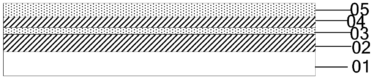
[0026] see figure 1 , a thin-film solar cell provided by an embodiment of the present invention includes: a substrate 01, a buffer layer disposed on the substrate 01, the buffer layer includes a zinc oxide thin film and a zinc sulfide thin film arranged overlappingly, wherein, as figure 1 As shown, the buffer layer at least includes: a first zinc oxide film layer 02, a first zinc sulfide film layer 03, a second zinc oxide film layer 04, and a second zinc sulfide film layer 05 sequentially arranged on the substrate 01; wherein, The content of oxygen atoms in the ...
Embodiment 1
[0104] The pulse sequence in the buffer layer preparation method is:
[0105] Step 1, forming a zinc oxide film layer through 60 ZnO pulse cycles;
[0106] Step 2, forming overlapping zinc oxide film layers and zinc sulfide film layers through 4 ZnO pulse cycles and 1 ZnS pulse cycle, and repeating the 4 ZnO pulse cycles and 1 ZnS pulse cycle for a total of 12 times, thereby passing 60 pulse cycles form zinc oxide film and zinc sulfide film;
[0107] Step 3, forming overlapping zinc oxide film layers and zinc sulfide film layers through 1 ZnO pulse cycle and 1 ZnS pulse cycle, and repeating the 1 ZnO pulse cycle and 1 ZnS pulse cycle for a total of 30 times, thereby passing 60 pulse cycles form zinc oxide film and zinc sulfide film;
[0108] Step 4, forming overlapping zinc oxide film layers and zinc sulfide film layers through 1 ZnO pulse cycle and 4 ZnS pulse cycles, and repeating the 1 ZnO pulse cycle and 4 ZnS pulse cycles for a total of 12 times, thereby passing 60 pul...
Embodiment 2
[0111] The pulse sequence in the buffer layer preparation method is:
[0112] Step 1, forming a zinc oxide film layer through 60 ZnO pulse cycles;
[0113] Step 2, forming overlapping zinc oxide film layers and zinc sulfide film layers through 9 ZnO pulse cycles and 1 ZnS pulse cycle, and repeating the 9 ZnO pulse cycles and 1 ZnS pulse cycle for a total of 6 times, thereby passing 60 pulse cycles form zinc oxide film and zinc sulfide film;
[0114] Step 3, forming overlapping zinc oxide film layers and zinc sulfide film layers through 1 ZnO pulse cycle and 1 ZnS pulse cycle, and repeating the 1 ZnO pulse cycle and 1 ZnS pulse cycle for a total of 30 times, thereby passing 60 pulse cycles form zinc oxide film and zinc sulfide film;
[0115] Step 4, forming overlapping zinc oxide film layers and zinc sulfide film layers through 1 ZnO pulse cycle and 9 ZnS pulse cycles, and repeating the 1 ZnO pulse cycle and 9 ZnS pulse cycles for a total of 6 times, thereby passing 60 pulse...
PUM
| Property | Measurement | Unit |
|---|---|---|
| Thickness | aaaaa | aaaaa |
Abstract
Description
Claims
Application Information
 - R&D
- Intellectual Property
- Life Sciences
- Materials
- Tech Scout
- Unparalleled Data Quality
- Higher Quality Content
- 60% Fewer Hallucinations
Browse by: Latest US Patents, China's latest patents, Technical Efficacy Thesaurus, Application Domain, Technology Topic, Popular Technical Reports.
© 2025 PatSnap. All rights reserved.Legal|Privacy policy|Modern Slavery Act Transparency Statement|Sitemap|About US| Contact US: help@patsnap.com