Bulk acoustic wave resonator integrated with fish-scale-shaped reflector array and processing method of bulk acoustic wave resonator
A technology of bulk acoustic wave resonators and mirror arrays, applied in electrical components, impedance networks, etc., can solve the problems of large anchor point loss, difficult application, low quality factor, etc., and achieve reduced mechanical reliability, good performance, and reduced acoustic waves. Effect
- Summary
- Abstract
- Description
- Claims
- Application Information
AI Technical Summary
Problems solved by technology
Method used
Image
Examples
Embodiment 1
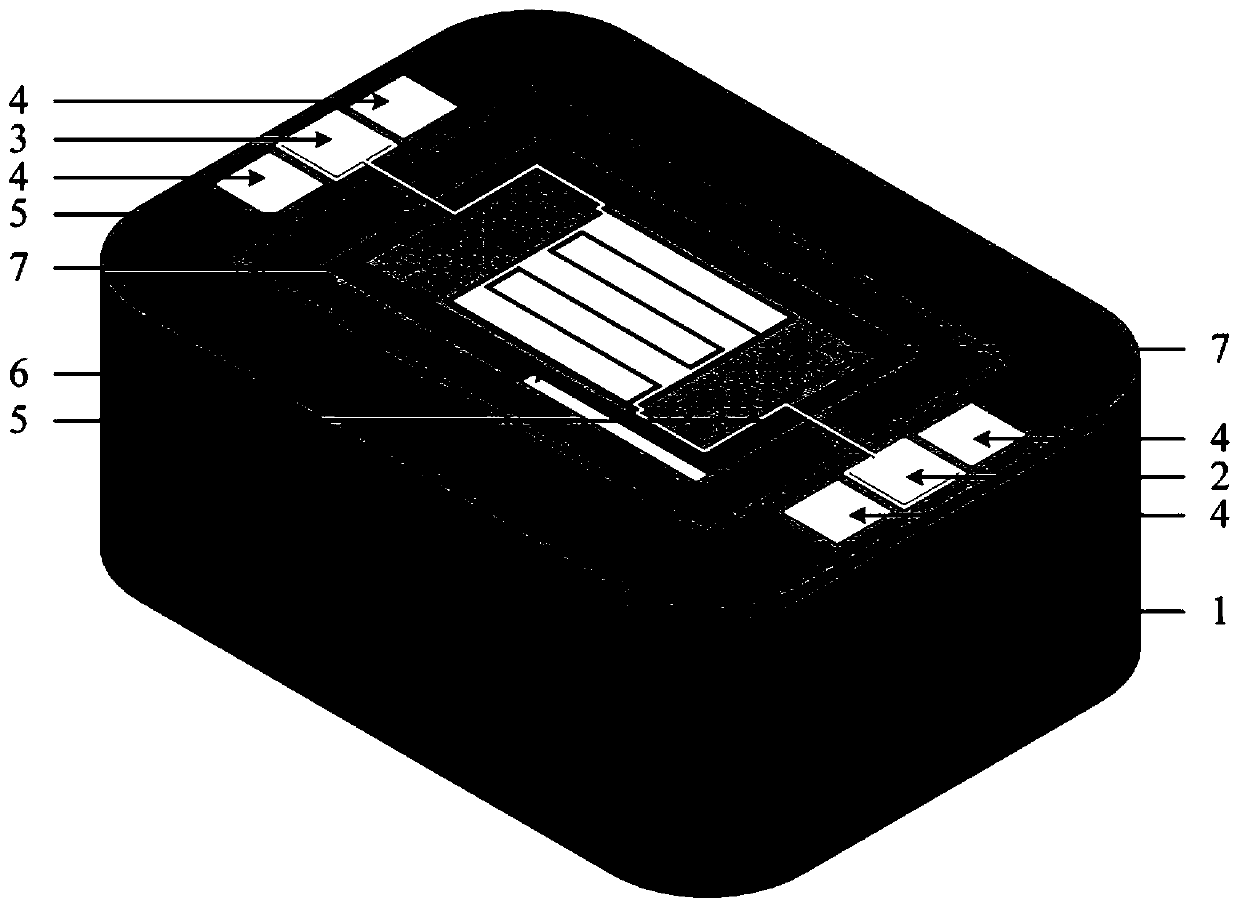
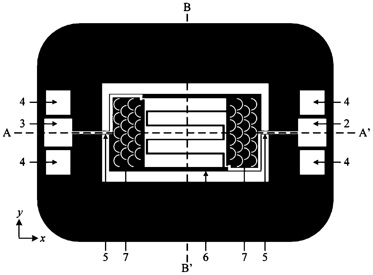
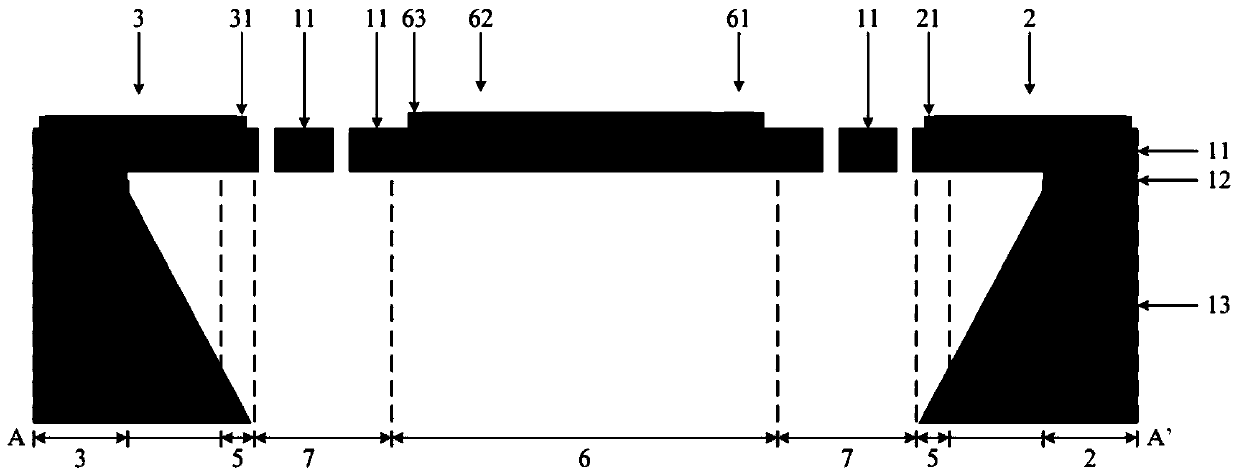
[0038] An embodiment of the present invention provides a bulk acoustic wave resonator integrated with a fish-scale reflector array, such as figure 1 and figure 2 As shown, it includes a SOI (Silicon-On-Insulator, silicon on insulator) substrate 1, an input electrode disk 2 located on the top of the SOI substrate 1, an output electrode disk 3, and a ground electrode disk 4, and is fixed and suspended on the SOI by a support beam 5. The resonator 6 at the center of the substrate 1, the fish scale mirror array 7 is integrated on both sides of the resonator 6; the input electrode disk 2 and the output electrode disk 3 are symmetrically arranged on both sides of the top of the SOI substrate 1, and the input electrode disk 2 and the output electrode disk Both sides of the electrode plate 3 are symmetrically provided with the ground electrode plate 4; the resonator 6 is suspended in the middle of the SOI substrate 1 by the support beam 5, and the interdigitated electrodes on the top...
Embodiment 2
[0054] An embodiment of the present invention provides a method for processing a bulk acoustic wave resonator integrated with a scale mirror array, such as Figure 7 As shown, the following steps S1-S9 are included:
[0055] S1. Select an SOI wafer with a crystal orientation, and set the top layer doped silicon with a thickness of 10±1 μm, the first buried oxide layer with a thickness of 1±0.05 μm, and the back layer with a thickness of 400±5 μm from top to bottom. Substrate silicon, get SOI substrate.
[0056] S2. Doping phosphorus into the doped silicon on the top layer of the SOI substrate to form a conductive layer, which serves as the ground layer of the entire bulk acoustic wave resonator.
[0057] S3, performing thermal oxidation on the top doped silicon to form 2000A 0 silicon dioxide, and obtain the second buried oxide layer of the contact part between the electrode plate and the top-layer doped silicon and the contact part between the metal wiring and the top-laye...
PUM
 Abstract
Description
Claims
Application Information


