Electric conduction coating material, plating solution, and PCB circuit board and production method thereof

A technology of conductive paint and plating solution, applied in conductive paint, printed circuit manufacturing, printed circuit and other directions, can solve the problems of large investment in production equipment, high production technology requirements, and large plant area, to simplify the production process, shorten the The effect of production cycle and total cost reduction

Inactive Publication Date: 2019-11-19
广东华祐新材料有限公司
View PDF8 Cites 0 Cited by
  • Summary
  • Abstract
  • Description
  • Claims
  • Application Information

AI Technical Summary

Problems solved by technology
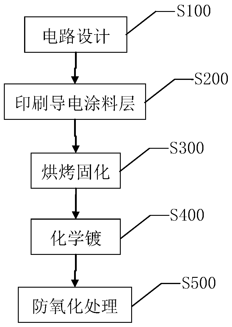
[0003] 1. The process is cumbersome and the production efficiency is not high;
[0004] 2. High production technology requirements, difficult production and high cost;
[0005] 3. A lot of investment in production equipment, occupying a large area of ​​the factory building, etc.

Method used


Image

  • Electric conduction coating material, plating solution, and PCB circuit board and production method thereof
  • Electric conduction coating material, plating solution, and PCB circuit board and production method thereof

Examples


example 1

[0052]Preparation of conductive coating: first take by weight 20% of phenolic resin, 5% of dicyandiamide, 69% of conductive copper powder, 1% of divalent ester solvent, 3.5% of tetramethylbenzene solvent, polyacrylate block copolymer dispersed Agent 1%, silicone defoamer 0.1%, leveling agent 0.4%; then add the phenolic resin, divalent ester solvent, tetramethylbenzene solvent and polyacrylate block copolymer dispersant into the plastic tank Finally, use a disperser to stir and disperse for 2H at a speed of 1000rpm to fully mix the phenolic resin, divalent ester solvent, tetramethylbenzene solvent and polyacrylate block copolymer dispersant; then add dicyandiamide curing agent and Stir and disperse at a high speed for 10 minutes to fully mix the dicyandiamide curing agent with the uniformly mixed phenolic resin, divalent ester solvent, tetramethylbenzene solvent and polyacrylate block copolymer dispersant; finally add conductive copper powder, The leveling agent and defoamer we...

example 2

[0057] Preparation of conductive coating: first take by weight 15% of epoxy resin, 5% of dicyandiamide, 75% of conductive copper powder, 1% of divalent ester solvent, 2.5% of tetramethylbenzene solvent, polyacrylate block copolymer Dispersant 1%, organosilicon defoamer 0.1% and leveling agent 0.4%; Then the phenolic resin, divalent ester solvent, tetramethylbenzene solvent and polyacrylate block copolymer dispersant will be weighed and added to the plastic tank After inside, use a disperser to stir and disperse for 2 hours at a speed of 1000rpm to fully mix the phenolic resin, divalent ester solvent, tetramethylbenzene solvent and polyacrylate block copolymer dispersant; then add dicyandiamide curing agent and Stir and disperse at a speed of 800rpm for 10 minutes to fully mix the dicyandiamide curing agent with the uniformly mixed phenolic resin, divalent ester solvent, tetramethylbenzene solvent and polyacrylate block copolymer dispersant; finally add conductive copper powder ...


PUM


Abstract

The invention relates to an electric conduction coating material, a plating solution, and a PCB circuit board and a production method thereof, wherein the electric conduction coating material is prepared from 5-75% of electric conduction copper powder, 15-20% of a resin, 5-10% of a curing agent, and 5-15% of an auxiliary agent, wherein the plating solution is prepared from of 1% of copper sulfate,1% of an alkali, 4.5-5.5% of potassium sodium tartrate, 0.1% of ethylenediaminetetraacetic acid, 1% of formaldehyde, and 91.4-92.4% of purified water. According to the present invention, the electricconduction coating material is directly silk-screened on the PCB circuit of a substrate, baking curing is performed, the obtained material is placed into the plating solution, the plated material istaken out, and anti-oxidation treatment is performed, such that the obtained PCB circuit board has an ultra-low-resistance electric-conduction coating and good conductivity while the production process is substantially simplified, the production difficulty is reduced, the production cycle is shortened, the total cost of the PCB circuit board is substantially reduced, the market competitiveness isstrong, the production process is pollution-free, and the surrounding environment of the industrial zone can be substantially improved so as to benefit the people.

Description

technical field [0001] The invention belongs to the technical field of PCB circuit boards and conductive materials, and in particular relates to a conductive coating, a plating solution, a PCB circuit board and a method for manufacturing a PCB circuit board. Background technique [0002] At present, the existing PCB circuit board manufacturers all use the subtractive method to produce PCB boards, but the applicant found that the traditional subtractive method has the following problems and shortcomings. [0003] 1. The process is cumbersome and the production efficiency is not high; [0004] 2. High production technology requirements, difficult production and high cost; [0005] 3. The investment in production equipment is large, and the workshop area is large. Contents of the invention [0006] In order to solve the above-mentioned problems in the prior art, the present invention provides a method that can be directly screen-printed on the substrate, which greatly simpl...

Claims


Application Information

Patent Timeline
Patent Type & Authority Applications(China)
IPC IPC(8): C09D161/06C09D163/00C09D5/24H05K1/09H05K3/12C23C18/40
CPCC08K2003/085C09D5/24C09D161/06C09D163/00C23C18/405H05K1/092H05K3/1216C08K3/08
Inventor 梁海
Owner 广东华祐新材料有限公司
Why Eureka
Try Eureka