

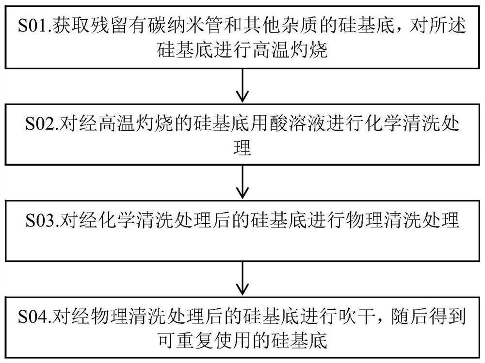
A method for cleaning a silicon substrate
A silicon substrate and physical cleaning technology, which is applied in the manufacture of electrical components, circuits, semiconductors/solid-state devices, etc., can solve the problems of poor cleaning effect of residues at the root of carbon nanotubes, easy corrosion of oxide layers, etc., and achieve extreme spinning performance Good, low yield, highly uniform results
- Summary
- Abstract
- Description
- Claims
- Application Information
AI Technical Summary
Problems solved by technology
Method used
Image


Examples
Embodiment 1
[0062] Obtain 200 8-inch silicon substrates with residual carbon nanotubes and other impurities, and use high-temperature burning for processing. Specifically, the silicon substrate after carbon nanotube growth was placed in an oven, and the high-temperature burning temperature was set to 650° C., and the burning treatment was performed for 2 minutes. The silicon substrate burned at high temperature is chemically cleaned with an acid solution, the acid solution is an SPM acid solution, and the cleaning treatment is carried out at a temperature of 110° C. for 15 minutes. Wherein, the SPM acid solution is a mixed solution of concentrated sulfuric acid and hydrogen peroxide, the mass concentration of the concentrated sulfuric acid is 95-98%, the mass concentration of the hydrogen peroxide is 25-35%, and the concentrated The volume ratio of sulfuric acid and the hydrogen peroxide is 40:1. Perform physical cleaning on the silicon substrate after chemical cleaning, first wash and r...
Embodiment 2
[0064]Obtain 200 8-inch silicon substrates with residual carbon nanotubes and other impurities, and use high-temperature burning for processing. Specifically, the silicon substrate after carbon nanotube growth was placed in an oven, and the high-temperature burning temperature was set to 600° C., and the burning treatment was performed for 3 minutes. The high-temperature-treated silicon substrate is chemically cleaned with an acid solution, the acid solution is an HPM acid solution, and the cleaning treatment is carried out at a temperature of 70° C. for 15 minutes. Wherein, the HPM acid solution is a mixed solution of deionized water, hydrogen peroxide, and hydrochloric acid, the mass concentration of the hydrogen peroxide is 25-35%, the mass concentration of the hydrochloric acid is 30-35%, and the mixed solution contains The volume ratio of the deionized water, the hydrogen peroxide, and the hydrochloric acid is 5:1:1. Physically clean the silicon substrate after chemical ...
Embodiment 3
[0066] Obtain 200 8-inch silicon substrates with residual carbon nanotubes and other impurities, and use high-temperature burning for processing. Specifically, the silicon substrate after carbon nanotube growth is placed in an oven, and the high-temperature burning temperature is set to 700° C., and the burning treatment is performed for 1 minute. The silicon substrate burned at high temperature is chemically cleaned with an acid solution, the acid solution is a hydrochloric acid solution, and the cleaning treatment is carried out at a temperature of 70° C., and the treatment time is 15 minutes. Wherein, the hydrochloric acid solution is a hydrochloric acid solution with a mass concentration of 20-35%. Perform physical cleaning on the silicon substrate after chemical cleaning, first wash and rinse with pure water for 6 minutes, and then scrub with a flat-panel cleaning machine. The specific steps are to take the silicon wafer out of the net bag and place it horizontally On th...
PUM
 Abstract
Description
Claims
Application Information