A lateral trench type insulated gate bipolar transistor and its preparation method

A bipolar transistor and lateral trench technology, used in semiconductor/solid-state device manufacturing, semiconductor devices, electrical components, etc., can solve the problems of reduced on-voltage drop, long off-time, current tailing, etc., to reduce saturation Effects of current density, increased forward blocking voltage, and reduced turn-off loss

Active Publication Date: 2021-06-08
UNIV OF ELECTRONICS SCI & TECH OF CHINA
View PDF7 Cites 0 Cited by
  • Summary
  • Abstract
  • Description
  • Claims
  • Application Information

AI Technical Summary

Problems solved by technology

When the device is conducting forward conduction, the holes injected by the collector junction enter the drift region, the parasitic pnp transistor is turned on, the conductance modulation is generated in the drift region, and the turn-on voltage drop is reduced; and due to the large injection effect, it takes a lot of time for the device to turn off Extract excess carriers, resulting in longer turn-off time, and serious current tailing phenomenon, which will cause greater turn-off loss in use

Method used


Image

  • A lateral trench type insulated gate bipolar transistor and its preparation method
  • A lateral trench type insulated gate bipolar transistor and its preparation method
  • A lateral trench type insulated gate bipolar transistor and its preparation method

Examples


Embodiment 1

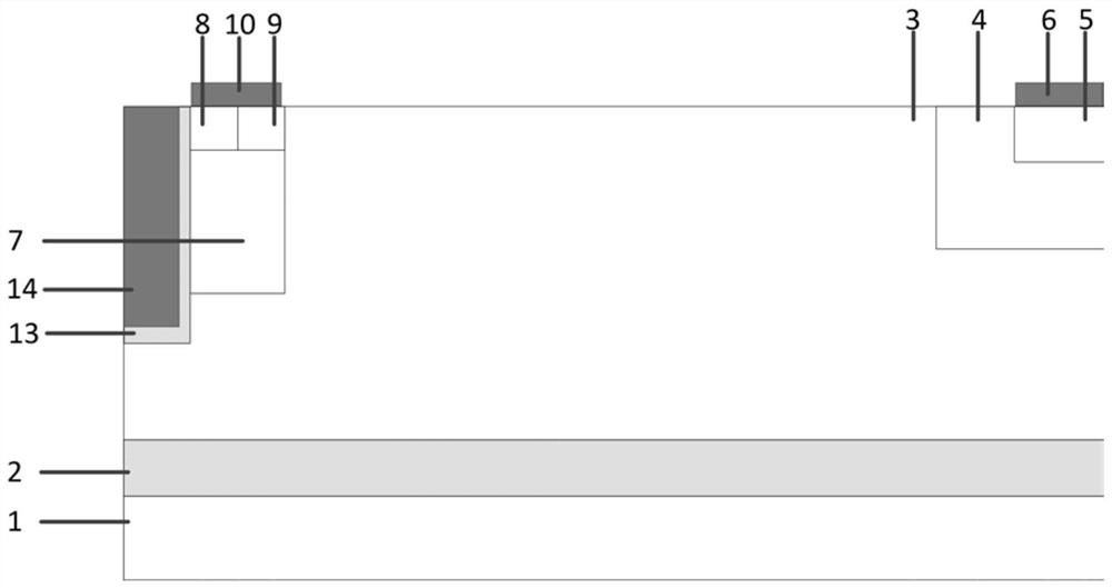
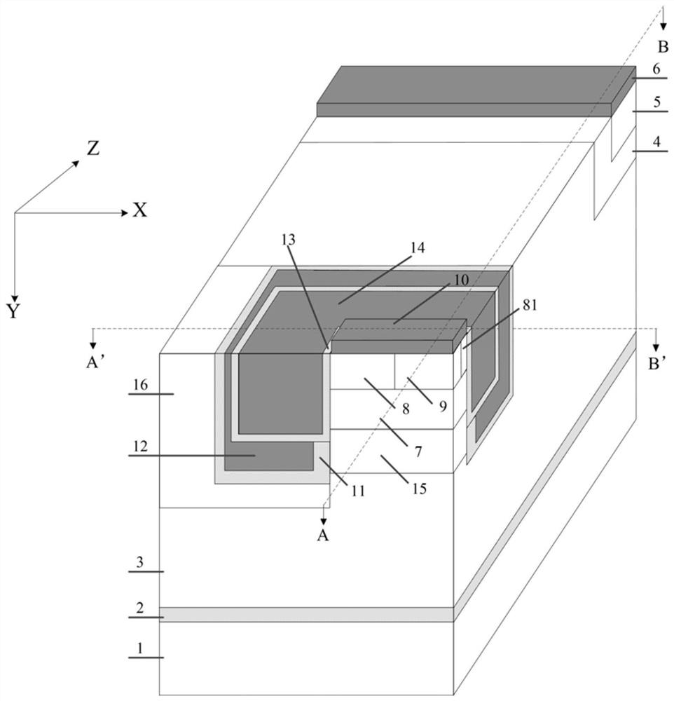
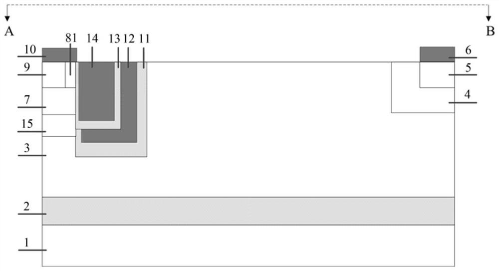
[0057] This embodiment provides a lateral insulated gate bipolar transistor, the half-cell structure of which is as follows figure 2 As shown, the two-dimensional cross-sectional structure obtained along the dotted line AB in the semi-cellular structure is as follows image 3 shown. This embodiment includes a P-type substrate 1, a silicon dioxide isolation layer 2, and an N-type drift region 3 arranged in sequence from bottom to top; an N-type buffer zone 4 is arranged on one side of the top layer of the N-type drift region 3 in the longitudinal direction, so The longitudinal direction is the third dimension perpendicular to the horizontal and vertical directions of the device; the N-type buffer zone 4 is provided with an N-type collector region 5, and the upper surface of the N-type collector region 5 is provided with a first metallized collector 6; in the N-type drift region 3, a P-type base region 7 is arranged on the side away from the N-type buffer zone 4 in the longitu...

Embodiment 2

[0066] This embodiment provides a lateral insulated gate bipolar transistor, the half-cell structure of which is as follows Figure 4 shown. In this embodiment, on the basis of Embodiment 1, an N-type doped region 17 is provided on the side of the N-type drift region 3 close to the first silicon dioxide layer 11 in the longitudinal direction, and the doping concentration of the N-type doped region 17 is high. The doping concentration in the N-type drift region 3 ; the vertical depth of the N-type doped region 17 is less than or equal to the vertical depth of the gate oxide layer 11 .

[0067] In particular, the horizontal direction of the N-type doped region 17 can extend from the left border of the half cell to the left border of the gate oxide layer 11 or the right border of the half cell or any position between the two.

[0068] Compared with Embodiment 1, the existence of the N-type doped region 17 can make the drift region in the longitudinal direction of the second emit...

Embodiment 3

[0070] This embodiment provides a lateral insulated gate bipolar transistor, the cell structure of which is as follows Figure 5 As shown, its two-dimensional cross-sectional view along the dotted line CD in the figure is as Figure 6 shown. In this embodiment, on the basis of Embodiment 2, a third metallized emitter 18 is provided above the P-type shielding layer 16 , and the third metallized emitter 18 forms a Schottky contact with the P-type shielding layer 16 .

[0071] In particular, the longitudinal length of the third metallized emitter 18 is smaller than the longitudinal length of the P-type shielding layer 16 .

[0072] Compared with Embodiment 2, the third metallized emitter 18 forms a Schottky contact with the P-type shielding layer 16, and the potential of the P-type shielding layer 16 can be increased during forward conduction, creating a hole barrier to prevent holes from flowing into the P. The type base region 7 can optimize the distribution of carriers in th...


PUM

PropertyMeasurementUnit
thicknessaaaaaaaaaa
thicknessaaaaaaaaaa
thicknessaaaaaaaaaa

Abstract

The invention belongs to the technical field of power semiconductor devices, and relates to a lateral trench type insulated gate bipolar transistor and a manufacturing method thereof. On the basis of the LIGBT device structure, the present invention adds a carrier storage layer and a vertical groove gate structure, which can enhance the conductance modulation effect and reduce the conduction voltage drop of the device; the channels in the horizontal direction and the longitudinal direction can improve the channel Density, reduce the turn-on voltage drop; wrap the side of the gate with a separate gate connected to the emitter, thereby reducing the Miller capacitance, reducing the turn-off time, reducing the turn-off loss, and improving the forward conduction voltage drop and turn-off loss. At the same time, it can reduce the gate charge of the device and reduce the driving loss; optimize the compromise characteristics of the current drop rate (di / dt) and conduction loss (Eon); the floating area on the left side of the slot gate can be in the forward resistance The break-off withstand voltage increases the blocking voltage, and at the same time allows a higher doping concentration of the carrier storage layer to reduce the on-voltage drop; the thick oxide layer at the bottom of the groove gate can increase the blocking voltage.

Description

technical field [0001] The invention belongs to the technical field of power semiconductors, in particular to a lateral trench type insulated gate bipolar transistor (IGBT). Background technique [0002] The lateral IGBT device is a horizontally integrated power device developed on the basis of the IGBT. It combines the advantages of the IGBT device structure, such as high input impedance, large conduction current, reduced conduction voltage, low power loss, and strong voltage blocking capability. , as the requirements for semiconductor integration become higher and higher, this kind of device that can maintain low power loss under high current will be more and more important in the field of horizontally integrated devices. [0003] As the feature size of integrated semiconductor devices continues to decrease, SOI technology has gradually become the mainstream technology for producing lateral IGBTs. SOI technology uses a buried oxide layer to isolate the top silicon from th...

Claims


Application Information

Patent Timeline
Patent Type & Authority Patents(China)
IPC IPC(8): H01L29/06H01L21/331H01L29/739
CPCH01L29/0611H01L29/66348H01L29/7393H01L29/7397
Inventor 张金平赵阳王康刘竞秀李泽宏张波
Owner UNIV OF ELECTRONICS SCI & TECH OF CHINA
Why Eureka
Try Eureka