Display panel and preparation method thereof

A display panel and substrate technology, which is applied in semiconductor/solid-state device manufacturing, electrical components, electrical solid-state devices, etc., can solve problems such as impedance rise, achieve the effect of increasing capacitance per unit area, meeting resolution requirements, and high-resolution requirements

Active Publication Date: 2019-12-13
SHENZHEN CHINA STAR OPTOELECTRONICS SEMICON DISPLAY TECH CO LTD
View PDF6 Cites 3 Cited by
  • Summary
  • Abstract
  • Description
  • Claims
  • Application Information

AI Technical Summary

Problems solved by technology

[0003] The present invention provides a display panel to solve the technical problem that the conductive part of the semiconductor layer has increased impedance when the subsequent thermal process time increases

Method used


Image

  • Display panel and preparation method thereof
  • Display panel and preparation method thereof
  • Display panel and preparation method thereof

Examples


Embodiment Construction

[0045] The following descriptions of the various embodiments refer to the accompanying drawings to illustrate specific embodiments in which the invention may be practiced. The directional terms mentioned in the present invention, such as [top], [bottom], [front], [back], [left], [right], [inside], [outside], [side], etc., are only for reference The orientation of the attached schema. Therefore, the directional terms used are used to illustrate and understand the present invention, but not to limit the present invention. In the figures, structurally similar elements are denoted by the same reference numerals.

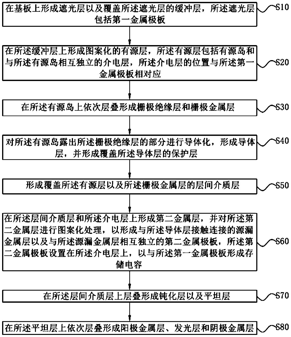
[0046] The invention aims at the technical problem that in the existing display panel, when the subsequent thermal process time increases, the impedance of the conductorized part of the semiconductor layer increases. The present invention can solve the above-mentioned problems.

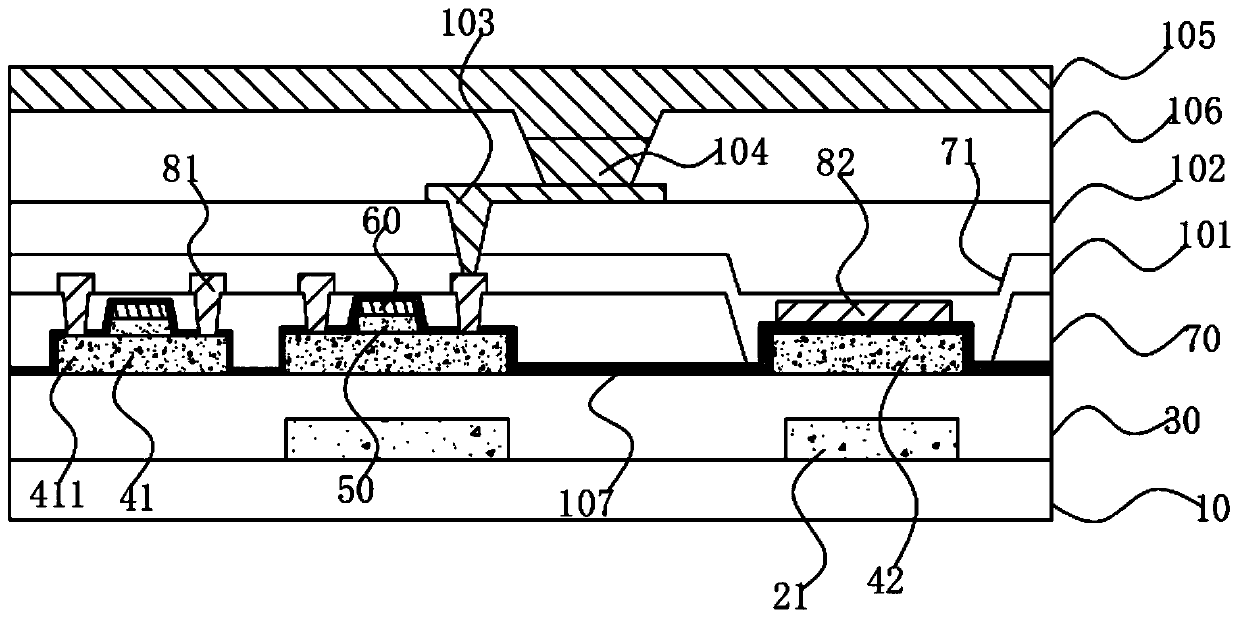
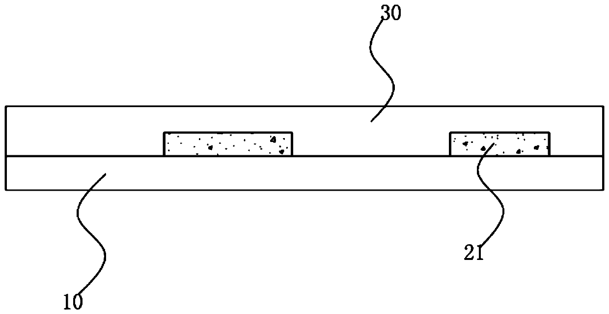
[0047] A display panel such as figure 1 As shown, it includes a substrate 10, a light-sh...


PUM


Abstract

The invention provides a display panel and a preparation method thereof. The display panel comprises a substrate, a shading layer arranged on the substrate, a buffer layer covering the shading layer,an active layer arranged on the buffer layer, a gate insulating layer, a gate metal layer, an interlayer dielectric layer and a second metal layer arranged on the interlayer dielectric layer, whereinthe gate insulating layer and the gate metal layer are stacked on the active layer, the interlayer dielectric layer is arranged on the buffer layer and covers the gate metal layer; the active layer comprises an active island, the active island comprises a conductor layer and a semiconductor layer which corresponds to and is in contact with the gate insulating layer, and the conductor layer is provided with a protective layer. The aluminum oxide protective layer with a compact structure is generated on the surface of the conductor layer by utilizing a mutual diffusion effect of aluminum atoms and oxygen atoms in the indium gallium zinc oxide, so that the conductor layer after conductor formation is protected, and the conductor layer is prevented from being influenced by the subsequent manufacturing process; and meanwhile, the aluminum oxide has the characteristic of high resistance, so that the capacitance per unit area of the storage capacitor can be effectively improved, and the requirement of high resolution is met.

Description

technical field [0001] The invention relates to the field of display technology, in particular to a display panel and a preparation method thereof. Background technique [0002] In the display panel industry, in the current Oxide TFT (Oxide Thin Film Transistor), part of the semiconductor layer made of IGZO (indium gallium zinc oxide, indium gallium zinc oxide) is conductorized. When the subsequent thermal process time increases, the semiconductor layer There is a problem of increased impedance in the conductorized part. Contents of the invention [0003] The invention provides a display panel to solve the technical problem that the resistance of the conductorized part of the semiconductor layer increases when the subsequent thermal process time increases. [0004] In order to solve the above problems, the technical solutions provided by the present invention are as follows: [0005] A display panel, comprising: [0006] Substrate; [0007] a light-shielding layer disp...

Claims


Application Information

Patent Timeline
Patent Type & Authority Applications(China)
IPC IPC(8): H01L27/12H01L27/32H01L21/77
CPCH01L27/1225H01L27/1255H01L27/1259H10K59/1213H10K59/1216H10K59/1201H01L29/78633H01L27/1248H10K59/126H01L21/385H01L27/156H10K59/124
Inventor 肖辉
Owner SHENZHEN CHINA STAR OPTOELECTRONICS SEMICON DISPLAY TECH CO LTD
Why Eureka
Try Eureka