Nested three-dimensional trench electrode silicon detector
A grooved electrode and nested technology, which is applied in the direction of circuits, electrical components, semiconductor devices, etc., can solve the problems of inconvenient adjustment of the size of the detector unit structure, limited practicability, limited sensitivity, etc., and achieve particle absorption performance And the effect of sensitivity improvement, wide application, and reduction of dead zone area
- Summary
- Abstract
- Description
- Claims
- Application Information
AI Technical Summary
Problems solved by technology
Method used
Image

Examples
Embodiment 1
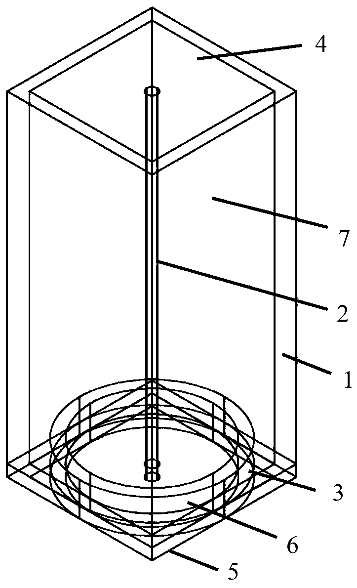
[0025] Nested 3D trench electrode silicon detectors, such as Figure 2-4 As shown, the bottom layer is a silicon dioxide protective layer 5, and the thickness of the silicon dioxide protective layer 5 is 1 μm; a peripheral electrode 1 is arranged on the silicon dioxide protective layer 5, and a height of 30 μm is embedded in the peripheral electrode 1. The nested part 3, the nested part 3 is composed of a p-type silicon substrate 6 located on the upper surface of the silicon dioxide layer 5 and an n-type heavily doped phosphorus silicon layer and a p-type lightly doped borosilicate layer located on the upper surface of the p-type silicon substrate 6 layer; the height of the p-type silicon substrate 6 is 10 μm, the length and width of the p-type silicon substrate 6 are equal to the outer length and outer width of the peripheral electrode 1, and the height of the n-type heavily doped phosphorus silicon layer and the p-type lightly doped borosilicate layer The center electrode 2 ...
Embodiment 2
[0027] Nested 3D trench electrode silicon detectors, such as Figure 2-4As shown, the bottom layer is a silicon dioxide protective layer 5, and the thickness of the silicon dioxide protective layer 5 is 1 μm; a peripheral electrode 1 is arranged on the silicon dioxide protective layer 5, and a height of 30 μm is embedded in the peripheral electrode 1. The nested part 3, the nested part 3 is composed of a p-type silicon substrate 6 located on the upper surface of the silicon dioxide layer 5 and an n-type heavily doped phosphorus silicon layer and a p-type lightly doped borosilicate layer located on the upper surface of the p-type silicon substrate 6 layer; the height of the p-type silicon substrate 6 is 20 μm, the length and width of the p-type silicon substrate 6 are equal to the outer length and outer width of the peripheral electrode 1, and the height of the n-type heavily doped phosphorus silicon layer and the p-type lightly doped borosilicate layer The center electrode 2 i...
Embodiment 3
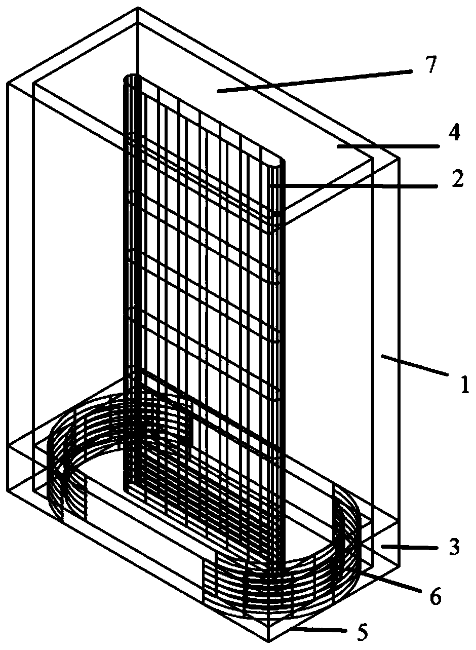
[0029] Nested 3D trench electrode silicon detectors, such as figure 1 As shown, the bottom layer is a silicon dioxide protective layer 5, and the thickness of the silicon dioxide protective layer 5 is 1 μm; on the silicon dioxide protective layer 5, a hollow cylinder nesting part 3 with equal length and a rectangular parallelepiped peripheral electrode are arranged. 1; the nested part 3 is composed of a p-type silicon substrate 6 located on the silicon dioxide protective layer 5 and an n-type heavily doped phosphorus silicon layer and a p-type lightly doped borosilicate layer located on the p-type silicon substrate 6; The height of the sleeve part 3 is 30 μm, the height of the p-type silicon substrate 6 is 25 μm, the length and width of the p-type silicon substrate 6 are equal to the outer length and outer width of the peripheral electrode 1, and the n-type heavily doped phosphorus silicon layer and the p-type lightly doped The height of the borosilicate layer is 5 μm; the cen...
PUM
| Property | Measurement | Unit |
|---|---|---|
| Thickness | aaaaa | aaaaa |
| Height | aaaaa | aaaaa |
| Height | aaaaa | aaaaa |
Abstract
Description
Claims
Application Information
 - R&D
- Intellectual Property
- Life Sciences
- Materials
- Tech Scout
- Unparalleled Data Quality
- Higher Quality Content
- 60% Fewer Hallucinations
Browse by: Latest US Patents, China's latest patents, Technical Efficacy Thesaurus, Application Domain, Technology Topic, Popular Technical Reports.
© 2025 PatSnap. All rights reserved.Legal|Privacy policy|Modern Slavery Act Transparency Statement|Sitemap|About US| Contact US: help@patsnap.com