Multi-bit memory of semiconductor nano-array organic field-effect transistor and preparation method thereof
A field-effect transistor and nano-array technology, applied in the field of semiconductor nano-array organic field-effect transistor multi-bit memory and its preparation, can solve the problems of poor data stability, slow light response speed, difficult multi-level storage and the like, and achieve high response speed , the effect of low operating voltage and high storage density
- Summary
- Abstract
- Description
- Claims
- Application Information
AI Technical Summary
Problems solved by technology
Method used
Image

Examples
Embodiment 1
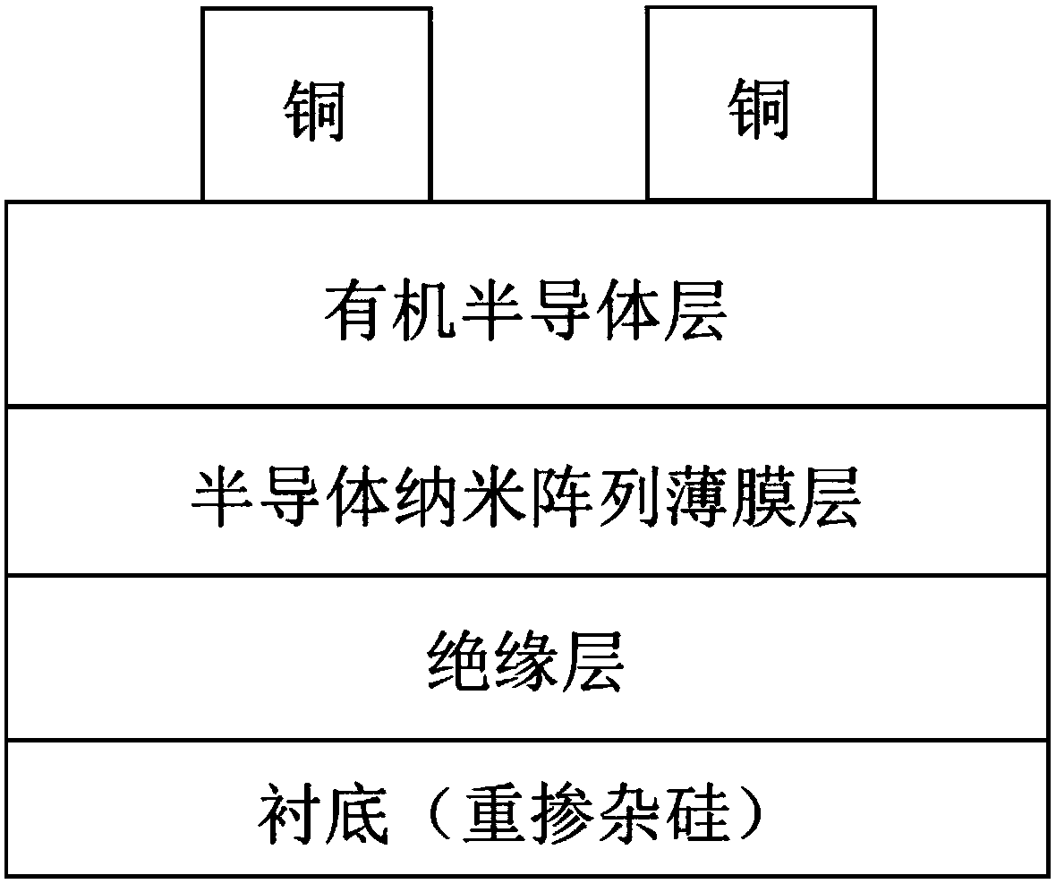
[0035] This embodiment provides an organic field effect transistor memory structure, the schematic diagram of which is as follows figure 1 shown, including:
[0036] substrate;
[0037] a gate electrode formed over the substrate;
[0038] a gate insulating layer covering the gate electrode;
[0039] a polymer film layer of a semiconductor nanoarray formed on the gate insulating layer;
[0040] an organic semiconductor layer formed on the semiconductor nanoarray thin film layer;
[0041] The source and drain electrodes are formed on both sides of the channel region on the surface of the organic semiconductor layer.
[0042] The substrate is a highly doped silicon wafer or a glass wafer or plastic PET.
[0043] In the technical solution of this embodiment, heavily doped silicon is used as the substrate and gate electrode; a layer of 50-300nm silicon dioxide is used as the gate insulating layer; the semiconductor nano-array is formed by mixed spin coating of polymer and semi...
Embodiment 2
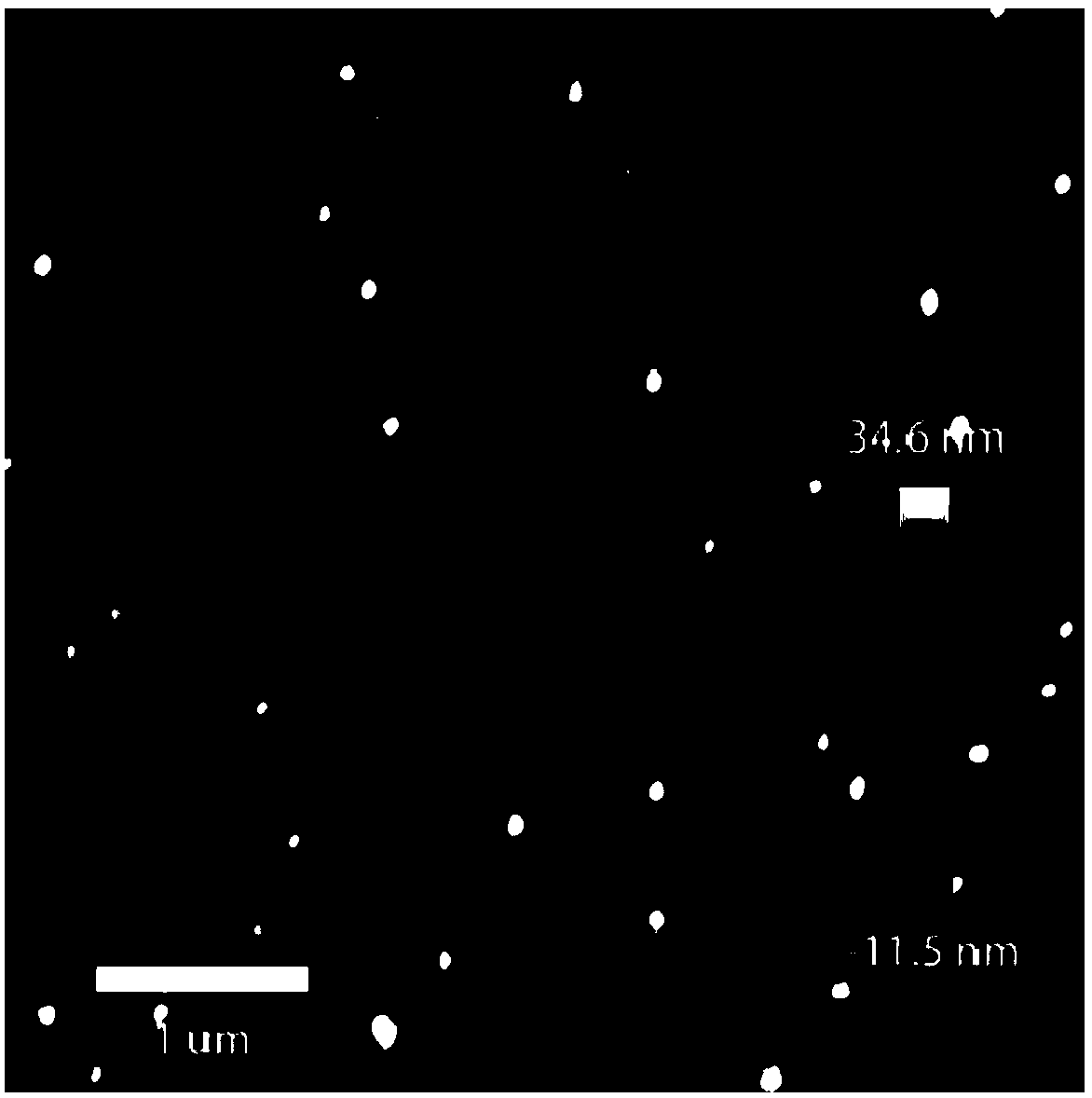
[0058] In the technical solution of this embodiment, heavily doped silicon is used as the substrate and gate electrode; a layer of 50-300 nm silicon dioxide is used as the gate insulating layer; the polymer film layer doped with semiconductor nanoparticles is made of polymer polymethyl Methyl acrylate (PMMA), semiconducting nanoparticles made of C 60 Preparation, the thickness after doping is 15-20 nm; a layer of 30-50 nm thick pentacene is vapor-deposited on the gate insulating layer to serve as an organic semiconductor layer; and metal copper is vapor-deposited on both sides of the conductive channel as source-drain electrodes.
[0059] (1) Prepare polymethyl methacrylate (PMMA) solution and C 60 solutions, the solution concentrations were 4 mg / mL and 0.6 mg / mL, respectively, and the solvent was toluene without additional treatment;
[0060] (2) Mix the solutions PS and C prepared in (1) 60 Mix at a ratio of 1:1 and sonicate for 30 minutes at a frequency of 100KHz;
[006...
Embodiment 3
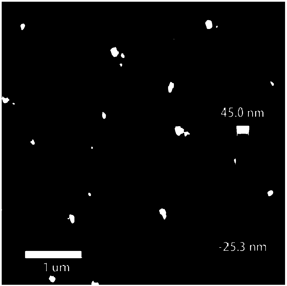
[0066] In the technical solution of this embodiment, heavily doped silicon is used as the substrate and gate electrode; a layer of 50-300 nm silicon dioxide is used as the gate insulating layer; the polymer film layer doped with semiconductor nanoparticles is made of polymer polyethylene Carbazole (PVK), semiconducting nanoparticles composed of C 60 Preparation, the thickness after doping is 15-20 nm; a layer of pentacene with a thickness of 30-50 nm is vapor-deposited on the gate insulating layer to serve as an organic semiconductor layer; and metal copper is vapor-deposited on both sides of the conductive channel as source-drain electrodes.
[0067] (1) Prepare polyvinylcarbazole (PVK) solution and C 60 solutions, the solution concentrations were 4 mg / mL and 0.6 mg / mL, respectively, and the solvent was toluene without additional treatment;
[0068] (2) Mix the solutions PS and C prepared in (1) 60 Mix at a ratio of 1:1 and sonicate for 30 minutes at a frequency of 100KHz; ...
PUM
| Property | Measurement | Unit |
|---|---|---|
| Thickness | aaaaa | aaaaa |
| Thickness | aaaaa | aaaaa |
| Thickness | aaaaa | aaaaa |
Abstract
Description
Claims
Application Information
 - R&D
- Intellectual Property
- Life Sciences
- Materials
- Tech Scout
- Unparalleled Data Quality
- Higher Quality Content
- 60% Fewer Hallucinations
Browse by: Latest US Patents, China's latest patents, Technical Efficacy Thesaurus, Application Domain, Technology Topic, Popular Technical Reports.
© 2025 PatSnap. All rights reserved.Legal|Privacy policy|Modern Slavery Act Transparency Statement|Sitemap|About US| Contact US: help@patsnap.com