Semiconductor structure and forming method thereof

A technology of semiconductor and gate structure, which is applied in the field of semiconductor structure and its formation, can solve the problems of high process difficulty, device performance and yield decline, etc., and achieve the effect of simplifying process steps, reducing adverse effects, and reducing process difficulty

Active Publication Date: 2019-12-31
SEMICON MFG INT (SHANGHAI) CORP +1
View PDF3 Cites 1 Cited by
  • Summary
  • Abstract
  • Description
  • Claims
  • Application Information

AI Technical Summary

Problems solved by technology

[0004] However, the current process of adjusting the threshold voltage is relatively difficult, and the adjustment of the threshold voltage may easily lead to a decline in device performance and yield.

Method used


Image

  • Semiconductor structure and forming method thereof
  • Semiconductor structure and forming method thereof
  • Semiconductor structure and forming method thereof

Examples


Embodiment Construction

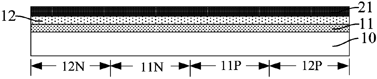
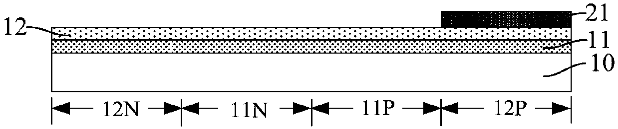
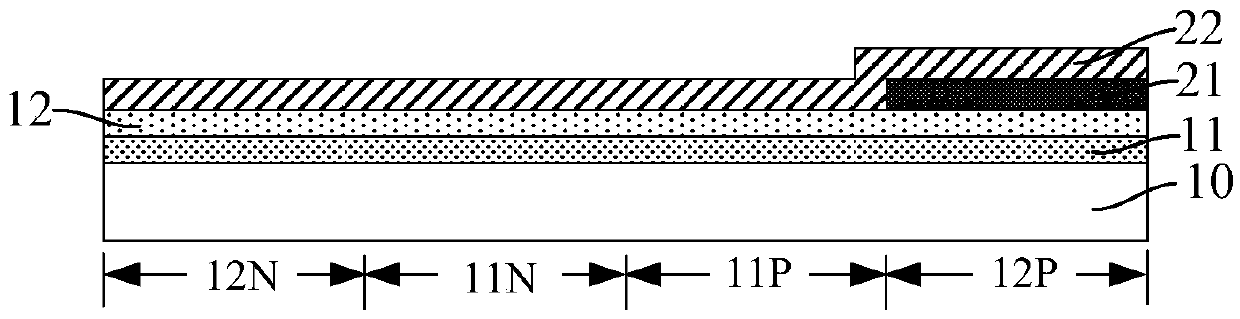
[0013] Lightly Doped Drain (LDD) implantation is the main process for accurately adjusting the threshold voltage of devices, but with the continuous reduction of the feature size of CMOS devices, the semiconductor process has gradually begun to shift from planar MOSFETs to three-dimensional three-dimensional ones with higher power efficiency. Transistor transitions such as Fin Field Effect Transistors (FinFETs). After the fin structure is introduced into the semiconductor structure, the effect of adjusting the threshold voltage of the device through the lightly doped drain implantation process will be correspondingly reduced. Therefore, at present, the multi-layer work function process (Multi-Work Function Process) is mainly used The NMOS device and the PMOS device have different threshold voltages.

[0014] In the multi-layer work function layer process, the doping ion concentration of the source and drain doping layers of each NMOS device is the same, and the doping ion conc...


PUM


Abstract

The invention discloses a semiconductor structure and a forming method thereof. The forming method comprises steps: a substrate is provided, wherein the types of the device regions comprise one or twoof an NMOS region and a PMOS region, and the same type of the device regions is used for forming devices with different threshold voltages; a gate structure is formed on the substrate; and source-drain doping layers are formed in the substrate at two sides of the gate structure, and in the same type of device regions, the source-drain doping layers corresponding to different threshold voltages have different doping ion concentrations. By adjusting the doping ion concentration of each source-drain doping layer in the same type of device regions, the threshold voltage of each device is easy toadjust respectively, the adverse effect of the process of forming a work function layer on the performance and yield of the device can be reduced, and the cross influence of the threshold voltage adjustment of any device on other devices is avoided.

Description

technical field [0001] The invention relates to the field of semiconductor manufacturing, in particular to a semiconductor structure and a forming method thereof. Background technique [0002] A Complementary Metal-Oxide Semiconductor (CMOS) device is one of the basic semiconductor devices constituting an integrated circuit. With the rapid development of integrated circuit manufacturing technology, the feature size of CMOS devices is always shrinking according to a certain ratio. It is a trend in the development of integrated circuits to replace the traditional oxide material gate dielectric layer with high-k material gate dielectric layer. . However, there are still many problems to be solved when forming a metal gate on a high-k gate dielectric layer, one of which is the matching of work function. Because the work function will directly affect the threshold voltage (Threshold Voltage, Vt) and device performance of the device, the work function must be adjusted to a suita...

Claims


Application Information

Patent Timeline
Patent Type & Authority Applications(China)
IPC IPC(8): H01L21/8238H01L27/092
CPCH01L21/8238H01L21/823814H01L27/092
Inventor 于书坤
Owner SEMICON MFG INT (SHANGHAI) CORP
Why Eureka
Try Eureka