An ultra-large bandwidth silicon-based waveguide mems optical switch

一种超大带宽、光开关的技术,应用在光波导光导、光学、光导等方向,能够解决不能满足高速大容量通信等问题,达到方便级联成光开关阵列、设计原理简单、插入损耗小的效果

Active Publication Date: 2020-08-14
ZHEJIANG UNIV
View PDF20 Cites 0 Cited by
  • Summary
  • Abstract
  • Description
  • Claims
  • Application Information

AI Technical Summary

Problems solved by technology

Traditional switches with electricity as the core can no longer meet the needs of high-speed and large-capacity communications, so people are gradually turning their attention to optical communications

Method used


Image

  • An ultra-large bandwidth silicon-based waveguide mems optical switch
  • An ultra-large bandwidth silicon-based waveguide mems optical switch
  • An ultra-large bandwidth silicon-based waveguide mems optical switch

Examples


Embodiment Construction

[0034] The present invention will be further described below in conjunction with drawings and embodiments.

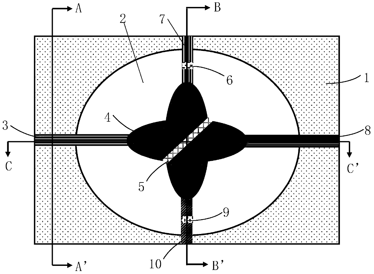
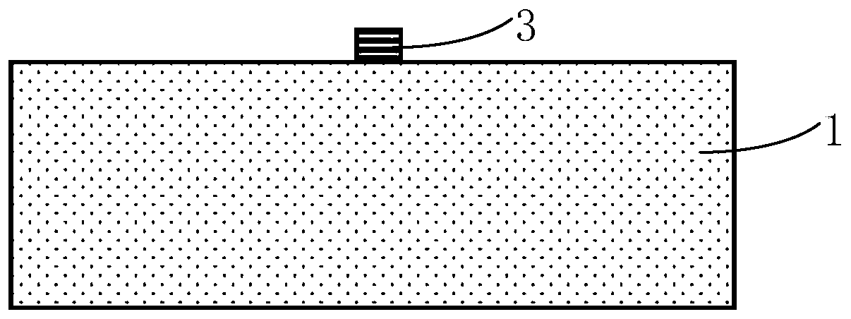
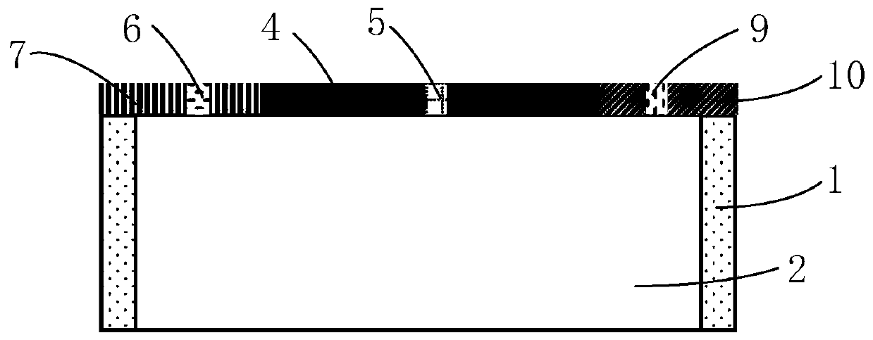
[0035] Such as figure 1 As shown, the specific implementation of the optical switch includes a silicon dioxide buried oxide layer 1, two input waveguides 3, 10 arranged on the silicon dioxide buried oxide layer 1, a cross waveguide 4 with nano-slopes, and two output waveguides The three parts of 7 and 8; the lower cladding layer of the whole device is made of silicon dioxide to form a silicon dioxide buried oxide layer 1, the upper cladding layer is air, and the lower cladding layer in the vicinity of the crossing waveguide is also air.

[0036] Such as Figure 1-Figure 4 As shown, the crossing waveguide 4 with nano-slant includes a crossing waveguide body and a nano-sloping groove 5 on the crossing waveguide body. The crossing waveguide body is composed of two elliptical cylinders with the same size and shape. The axial direction is perpendicular to the surface of th...


PUM

PropertyMeasurementUnit
refractive indexaaaaaaaaaa

Abstract

The invention discloses an ultra-large bandwidth silicon-based waveguide MEMS optical switch. The optical switch is mainly composed of three parts: input waveguide, cross waveguide with nano-slant groove, and output waveguide. The crossover waveguide is composed of two identical orthogonal elliptical cylinders. The four ports of the crossover waveguide respectively extend the single-mode strip waveguide as the input / output waveguide; The two waveguides are also fully etched with nano-grooves, which penetrate through the lower cladding layer near the cross-waveguide and the nano-groove. By adjusting the voltage applied to both ends of the cross-waveguide to adjust the width of the nano-chute, in this way the direct or full optical path reflection. The invention switches the propagation path of the optical switch by adjusting the voltage applied to the cross waveguide, has a simple structure, is convenient for integration and cascading, and is expected to realize an arrayed waveguide optical switch with miniaturization, low cost, and fast adjustment speed.

Description

technical field [0001] The invention relates to an ultra-large bandwidth silicon-based waveguide MEMS optical switch, in particular to an integrated silicon-based waveguide MEMS optical switch capable of controlling the light transmission direction by adding a bias voltage. Background technique [0002] Due to the rapid growth of data traffic and the increasing requirements for reconfigurability and scalability of data center networks, fast optical circuit switches in data center networks have been extensively studied. The traditional switch with electricity as the core can no longer meet the needs of high-speed and large-capacity communication, so people are gradually turning their attention to optical communication. Since the 1990s, optical communication has developed rapidly, and the status of optical interconnection and optical switches, which are key links in optical communication, has naturally become more and more important. [0003] Optical switches are key componen...

Claims


Application Information

Patent Timeline
Patent Type & Authority Patents(China)
IPC IPC(8): G02B6/10G02B6/12G02B6/136G02B26/00G02B26/08
CPCG02B6/107G02B6/12004G02B6/136G02B26/00G02B26/0833G02B2006/12145G02B6/3596G02B6/357G02B6/3506G02B6/3546G02B6/356
Inventor 戴道锌孙仪
Owner ZHEJIANG UNIV
Why Eureka
Try Eureka