Double-layer DMF chip rapidly prepared based on polymer composite film and preparation method

A composite membrane and polymer technology, applied in the field of microfluidics, can solve the problems of complex steps, surface grooves of the dielectric layer and hydrophobic layer, affecting the stability of droplet movement, etc., and achieves reduced manufacturing costs, simplified chip manufacturing steps, The effect of reducing the cost of experiments

Active Publication Date: 2020-01-10
ZHEJIANG UNIV
View PDF12 Cites 3 Cited by
  • Summary
  • Abstract
  • Description
  • Claims
  • Application Information

AI Technical Summary

Problems solved by technology

The traditional chip consists of two different materials, the dielectric layer and the hydrophobic layer. The preparation process of each layer usually adopts the spin coating process, which has complicated steps, and if the thickness of the electrode is too large, it will cause "grooves" on the surface of the dielectric layer and the hydrophobic layer. This affects the stability of the droplet motion

Method used


Image

  • Double-layer DMF chip rapidly prepared based on polymer composite film and preparation method
  • Double-layer DMF chip rapidly prepared based on polymer composite film and preparation method
  • Double-layer DMF chip rapidly prepared based on polymer composite film and preparation method

Examples


Embodiment Construction

[0038] Below in conjunction with accompanying drawing of description, the present invention is described further, but the present invention is not limited to following examples.

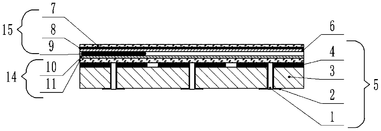
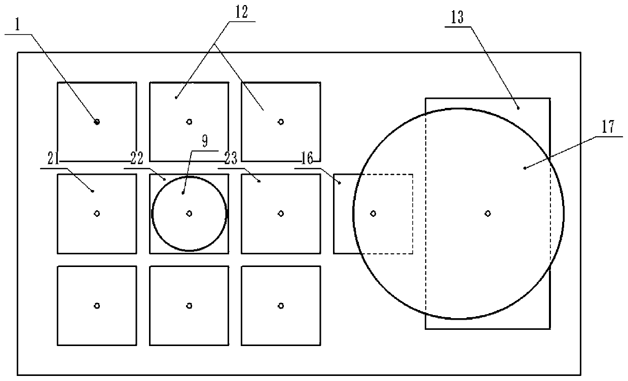
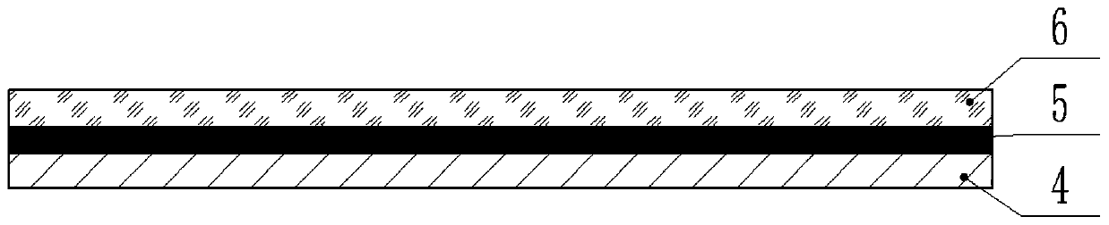
[0039] Such as figure 1 As shown, including the lower pole plate 5 and the upper pole plate 15, such as image 3 As shown, the upper pole plate 15 is mainly composed of the upper pole plate hydrophobic layer 6, the upper pole plate substrate 7 and the upper pole plate conductive layer 8 sequentially stacked from bottom to top; The electrode array layer, the large electrode layer, the dielectric layer 11 and the lower plate hydrophobic layer 10, the dielectric layer 11 includes a polymer composite film substrate layer and a polymer composite film adhesive layer that are stacked from top to bottom; The electrical layer 11 and the hydrophobic layer 10 of the lower plate are sequentially arranged on the electrode layer, and the dielectric layer 11 is located between the hydrophobic layer 10 of the lower...


PUM

PropertyMeasurementUnit
thicknessaaaaaaaaaa

Abstract

The invention discloses a double-layer DMF chip rapidly prepared based on a polymer composite film and a preparation method. The double-layer DMF chip rapidly prepared based on a polymer composite film comprises a lower layer polar plate, and an upper layer polar plate; the upper layer polar plate comprises an upper layer hydrophobic layer, a substrate and a conductive layer; the lower layer polarplate comprises an electrode layer, a dielectric layer and a lower layer polar plate hydrophobic layer; the dielectric layer comprises a polymer composite film base material layer and a polymer composite film adhesive layer; the electrode layer comprises an electrode array layer and a large electrode layer; a liquid storage zone is provided with the large electrode layer, and a motion zone is provided with the electrode array layer; the large electrode layer comprises large electrodes and small electrodes; the electrode array layer comprises a printed circuit board substrate and an electrodearray; circuit board through holes are formed in the middles of all driving electrode units, the small electrodes and the large electrodes, and bonding pads are arranged around the through holes; andreagent liquid drops are arranged between the lower layer polar plate and the upper layer polar plate. According to a process provided by the invention, the preparation cost of digital microfluidic chips can be greatly reduced, the possibility of cross infection caused by adsorption of biological reagents on surfaces of materials is avoided, and the flexibility and stability of microfluidic control are improved.

Description

technical field [0001] The invention relates to a DMF chip and a preparation method in the field of microfluidics, in particular to a rapid preparation of a double-layer DMF chip based on a polymer composite film and a preparation method. Background technique [0002] At present, when relevant biochemical experiments are involved in the fields of drug development, disease detection, and genetic testing, experimenters are required to use tools such as pipettes, kits, and test tubes to conduct experiments. A large number of repeated steps and the use of experimental reagents cause a great waste of experimental resources. Microfluidic technology designs different channels on the chip to realize the mixed reaction function of the liquid. Combined with certain detection methods, the reaction and detection steps can be concentrated on one chip, and the volume of the reaction droplet is reduced to the nanoliter or even picoliter level. The change of the electric field of the chip ...

Claims


Application Information

Patent Timeline
Patent Type & Authority Applications(China)
IPC IPC(8): B01L3/00
CPCB01L3/502707B01L2300/165
Inventor 应义斌王振叶尊忠吴翠应圣纳
Owner ZHEJIANG UNIV
Why Eureka
Try Eureka