A method for making texture on silicon wafers by reusing black silicon cleaning solution

A cleaning fluid, black silicon technology, applied in the direction of final product manufacturing, sustainable manufacturing/processing, semiconductor/solid-state device manufacturing, etc., can solve problems such as high costs, achieve simple operation, reduce texturing costs and wastewater treatment costs, The effect of easy industrial production

Active Publication Date: 2021-09-28
INST OF PHYSICS - CHINESE ACAD OF SCI
View PDF5 Cites 0 Cited by
  • Summary
  • Abstract
  • Description
  • Claims
  • Application Information

AI Technical Summary

Problems solved by technology

However, in order to achieve the recovery and utilization of these metal ions, it is usually necessary to set up an additional metal recovery and treatment system, which requires high costs.

Method used


Image

  • A method for making texture on silicon wafers by reusing black silicon cleaning solution
  • A method for making texture on silicon wafers by reusing black silicon cleaning solution
  • A method for making texture on silicon wafers by reusing black silicon cleaning solution

Examples


Embodiment 1

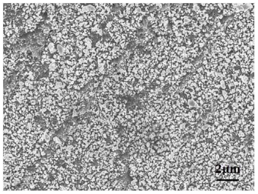
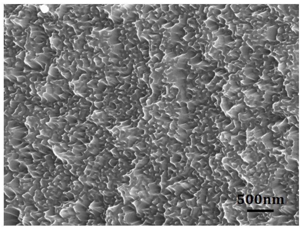
[0054] Step 1: Take a P-type diamond wire-cut polycrystalline silicon wafer (resistivity 1-3Ωcm) with a size of 156mm×156mm, and immerse it in the acidic black silicon texturing solution in the texturing tank for texturing. The reaction temperature is 25°C. The time is 5 minutes, and discretely distributed silver metal particles are formed on the surface of the silicon wafer; among them, the acidic black silicon texturing solution is prepared from silver nitrate, copper nitrate, hydrofluoric acid, nitric acid and deionized, with a total volume of 300L, nitric acid The concentration of silver was 0.5 mmol / L, the concentration of copper nitrate was 50 mmol / L, the concentration of hydrofluoric acid was 3 mol / L, and the concentration of nitric acid was 4 mol / L.

[0055] Step 2: Take out the textured silicon wafer obtained in Step 1, wash it with deionized water, and dry it with high-purity nitrogen.

[0056] Step 3: Wash the dried silicon chip obtained in step 2 with black silicon...

Embodiment 2

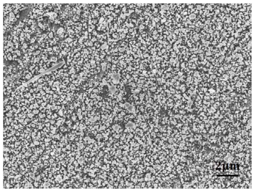
[0065] Step 1: Take a P-type diamond wire cut polysilicon wafer (resistivity 1-3Ωcm) with a size of 156mm×156mm, and immerse it in the acidic black silicon texturing solution in the texturing tank for texturing. The reaction temperature is 30°C. The time is 5 minutes, and discretely distributed silver metal particles are formed on the surface of the silicon wafer; among them, the acidic black silicon texturing solution is prepared from silver nitrate, hydrofluoric acid, nitric acid and deionized, the total volume is 200L, and the concentration of silver nitrate is The concentration of hydrofluoric acid is 0.5mmol / L, the concentration of hydrofluoric acid is 4.5mol / L, and the concentration of nitric acid is 4mol / L.

[0066] Step 2: Take out the textured silicon wafer obtained in Step 1, wash it with deionized water, and dry it with high-purity nitrogen.

[0067] Step 3: Wash the dried silicon chip obtained in step 2 with black silicon cleaning solution to remove silver metal pa...


PUM

PropertyMeasurementUnit
sizeaaaaaaaaaa
sizeaaaaaaaaaa

Abstract

The invention discloses a method for making texture on a silicon chip by repeatedly using a black silicon cleaning solution, which includes: (1) immersing the silicon chip in a metal ion salt containing 0.01-200mmol / L and 1-10mol / L hydrogen fluorine Carry out texturing in the black silicon texturing liquid of acid and 0.1-10mol / L; (2) clean the silicon chip after making texturing with deionized water, dry; (3) adopt the nitric acid solution cleaning step of 20-80wt% ( 2) the dried silicon chip obtained in to remove the metal particles deposited on the surface of the silicon chip; (4) clean the silicon chip with deionized water after cleaning the black silicon cleaning solution, and dry it to obtain a suede structure and (5) repeating steps (1) to (4), until the black silicon cleaning solution reaches the service life, the black silicon cleaning solution that reaches the service life is used as a raw material to prepare the black silicon texturing solution. The method of the invention can simply and effectively realize the repeated utilization of the black silicon cleaning solution, especially the metal ions therein, reduces the cost of texturing and waste water treatment, and is environmentally friendly.

Description

technical field [0001] The invention relates to the field of semiconductors, in particular to a method for making texture on a silicon chip by repeatedly using a black silicon cleaning solution. Background technique [0002] Because of its large reserves and wide distribution, solar energy is of great significance to improving the existing energy structure. Solar power generation mainly uses solar cells to convert solar energy into electrical energy. Among them, silicon-based solar cells are currently the most widely used solar cells. Silicon-based solar cells mainly include monocrystalline silicon solar cells and polycrystalline silicon solar cells. [0003] At this stage, for monocrystalline silicon solar cells and polycrystalline silicon solar cells, diamond wire slicing technology can significantly reduce the cost of slicing silicon ingots, and ultimately reduce the cost of photovoltaic modules. However, the diamond wire slicing technology has not been fully applied i...

Claims


Application Information

Patent Timeline
Patent Type & Authority Patents(China)
IPC IPC(8): H01L21/02H01L21/306H01L31/18H01L31/0236
CPCH01L21/02057H01L21/30608H01L31/02363H01L31/1804Y02P70/50
Inventor 赵燕刘尧平王燕杜小龙朱姚培唐磊蒋健王磊
Owner INST OF PHYSICS - CHINESE ACAD OF SCI
Why Eureka
Try Eureka