
MOS-HEMT device containing multi-layer high-K gate insulating layer and preparation method of MOS-HEMT device

A MOS-HEMT, gate insulating layer technology, used in semiconductor/solid-state device manufacturing, semiconductor devices, electrical components, etc., can solve the problem of complex device preparation process, and achieve the goal of simplifying the preparation process, reducing leakage current, and increasing the K value. Effect

Pending Publication Date: 2020-01-17
中证博芯(重庆)半导体有限公司
View PDF0 Cites 0 Cited by
  • Summary
  • Abstract
  • Description
  • Claims
  • Application Information

AI Technical Summary

Problems solved by technology

[0003] In order to effectively suppress the gate current of compound HEMT devices in the prior art, there is currently a MOS-HEMT device formed by introducing a metal-oxide-semiconductor (MOS) structure, but the MOS structure to form a MOS-HEMT device will lead to device fabrication For the technical problem of relatively complicated process, the present invention provides a MOS-HEMT device containing multiple layers of high-K gate insulating layers

Method used


Image

  • MOS-HEMT device containing multi-layer high-K gate insulating layer and preparation method of MOS-HEMT device
  • MOS-HEMT device containing multi-layer high-K gate insulating layer and preparation method of MOS-HEMT device
  • MOS-HEMT device containing multi-layer high-K gate insulating layer and preparation method of MOS-HEMT device

Examples


Embodiment Construction

[0029] In order to make the technical means, creative features, goals and effects achieved by the present invention easy to understand, the present invention will be further described below in conjunction with specific illustrations.

[0030] In describing the present invention, it is to be understood that the terms "longitudinal", "radial", "length", "width", "thickness", "upper", "lower", "front", "rear", The orientation or positional relationship indicated by "left", "right", "vertical", "horizontal", "top", "bottom", "inner", "outer", etc. is based on the orientation or positional relationship shown in the drawings , is only for the convenience of describing the present invention and simplifying the description, but does not indicate or imply that the referred device or element must have a specific orientation, be constructed and operated in a specific orientation, and thus should not be construed as limiting the present invention. In the description of the present inventi...


PUM

PropertyMeasurementUnit
thicknessaaaaaaaaaa
thicknessaaaaaaaaaa
thicknessaaaaaaaaaa

Abstract

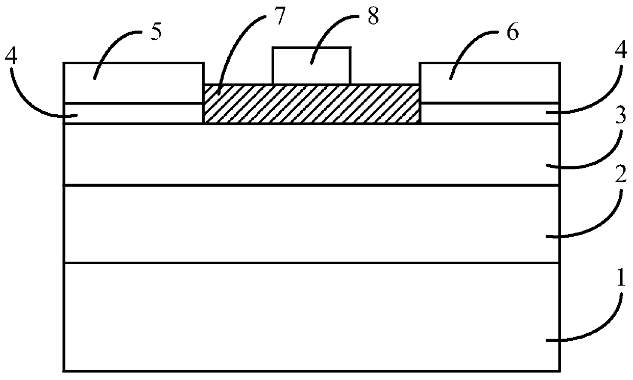
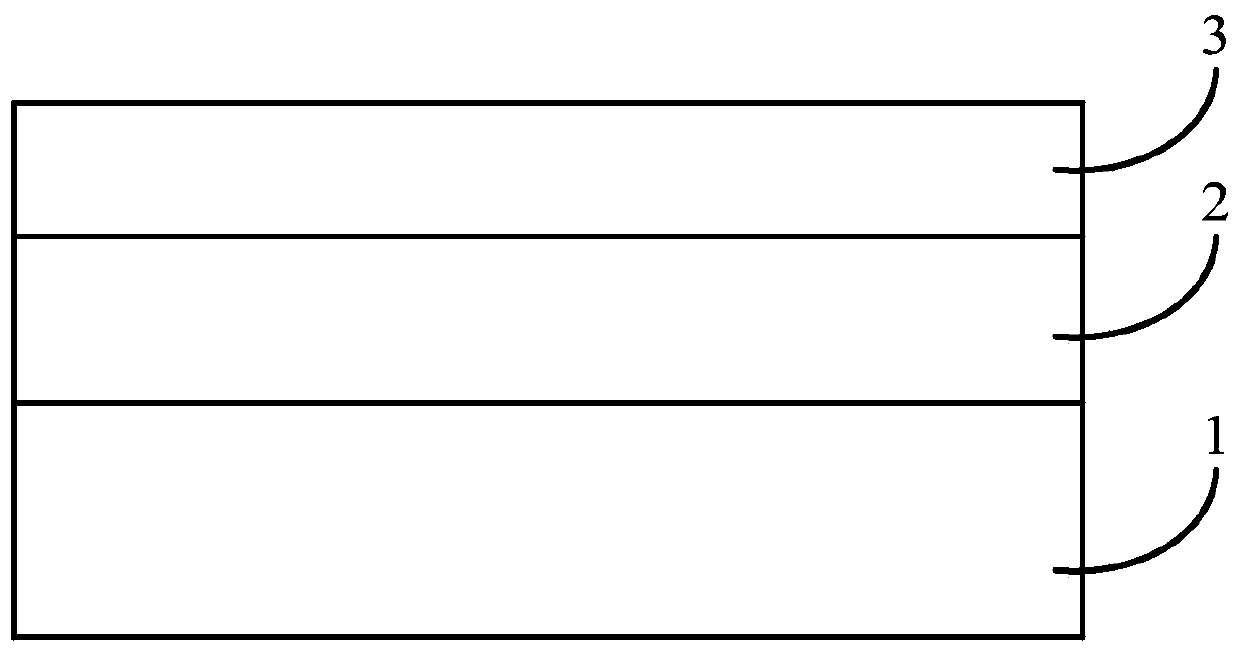
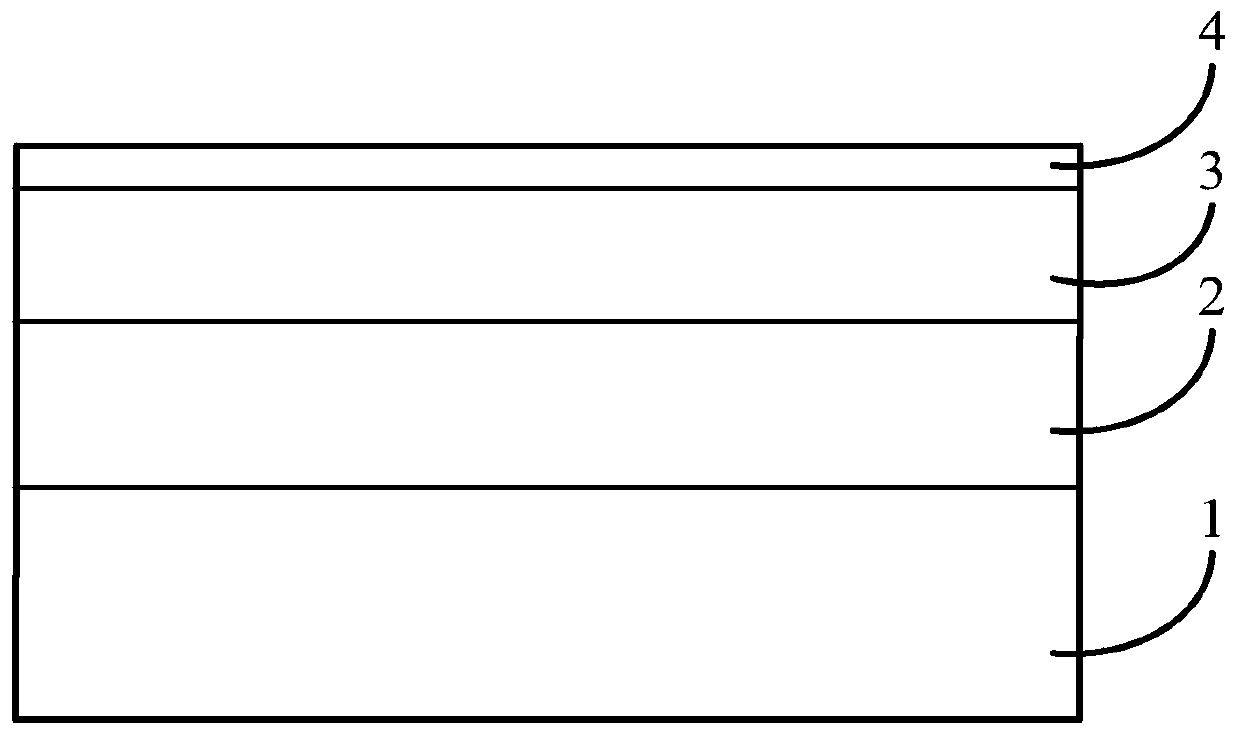
The invention provides an MOS-HEMT device containing a multi-layer high-K gate insulating layer . The device includes a substrate, wherein a buffer layer with the thickness of 1-2 microns, a barrier layer with the thickness of 25-30nm and an aluminum metal film are sequentially formed on the surface of the substrate; graphical source electrodes and drain electrodes are correspondingly formed on the surfaces of the aluminum metal films on the left and right sides of the surface of the barrier layer; a multi-layer high-K gate insulating layer is formed between the source and drain electrode channels; The multi-layer high-K gate insulating layer includes an aluminum oxide layer which is generated by directly oxidizing aluminum metal films between the aluminum metal films on the left side andthe right side of the surface of the barrier layer, a zirconium oxide layer which is formed on the surface of the aluminum oxide layer in an overlapped mode, the surface of the aluminum oxide layer isflush with the bottom faces of the source electrode and the drain electrode, and a gate electrode is formed on the surface of the zirconium oxide layer. The invention also provides a preparation method of the device. The multi-layer high-K gate insulating layer is formed by stacking the aluminum oxide and the zirconium oxide, so that the performance stability of the device can be improved, the possibility of deterioration of leakage current and key characteristics of the device is reduced, and the preparation method can be compatible with an existing HEMT device preparation process.

Description

technical field [0001] The invention relates to the technical field of semiconductors, in particular to a MOS-HEMT device containing multiple high-K gate insulating layers and a preparation method thereof. Background technique [0002] GaAs and GaN-based compound HEMT (High Electron Mobility Transistor, High Electron Mobility Transistor) semiconductor devices have the advantages of ultra-high frequency and high power, and currently have broad application prospects in the fields of wireless 5G communication and radar. However, the leakage problem of traditional Schottky gate HEMT devices is relatively serious, which easily leads to the deterioration of key performances such as breakdown voltage, efficiency, and gain of the device. In order to effectively suppress the gate current, it is an effective solution to introduce a metal-oxide-semiconductor (MOS) structure into the gate of the traditional compound HEMT structure to form a MOS-HEMT device. However, the inventors of th...

Claims


Application Information

Patent Timeline
Patent Type & Authority Applications(China)
IPC IPC(8): H01L29/423H01L29/51H01L29/778H01L21/28H01L21/336
CPCH01L29/7787H01L29/66462H01L29/401H01L29/42364H01L29/517H01L29/513
Inventor 李迈克
Owner 中证博芯(重庆)半导体有限公司
Features
  • Generate Ideas
  • Intellectual Property
  • Life Sciences
  • Materials
  • Tech Scout
  • Unparalleled Data Quality
  • Higher Quality Content
  • 60% Fewer Hallucinations
Learn More