Trench gate type silicon-on-insulator lateral insulated gate bipolar transistor device

A technology of silicon-on-insulator and bipolar transistors, which is applied to semiconductor devices, electrical components, circuits, etc., can solve the problems of lower device reliability, large leakage current, and increase of peak current of turn-on current, so as to improve control ability and low switching The effect of low loss and peak current

Active Publication Date: 2020-01-24
SOUTHEAST UNIV
View PDF6 Cites 0 Cited by
  • Summary
  • Abstract
  • Description
  • Claims
  • Application Information

AI Technical Summary

Problems solved by technology

However, in order to obtain a lower conduction voltage drop, the number of carriers stored in the drift region will be increased, and the peak current of the turn-on current will increase, which will cause gate overshoot when the device is turned on, causing the device to turn on. fault, the device is not safe to turn on
In addition, the switching speed of the SOI-LIGBT device is the bottleneck that restricts the monolithic integrated power chip to work at a higher frequency, with better energy efficiency and smaller chip area.
Therefore, in order to increase the turn-on speed of the device, some devices with improved structures have been proposed, such as SA-LIGBT and some devices after electron radiation. These structures can effectively increase the turn-on time and reduce the turn-off loss, but at the same time bring For example, the former will have voltage hysteresis during forward conduction, which will reduce the reliability of the device, while the latter may have a large leakage current at high temperature, resulting in unstable device performance

Method used


Image

  • Trench gate type silicon-on-insulator lateral insulated gate bipolar transistor device
  • Trench gate type silicon-on-insulator lateral insulated gate bipolar transistor device
  • Trench gate type silicon-on-insulator lateral insulated gate bipolar transistor device

Examples


Embodiment Construction

[0028] Combine below figure 2 , image 3 , Figure 4 and Figure 5 , the present invention is described in detail:

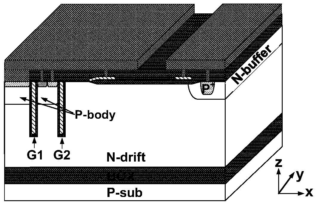
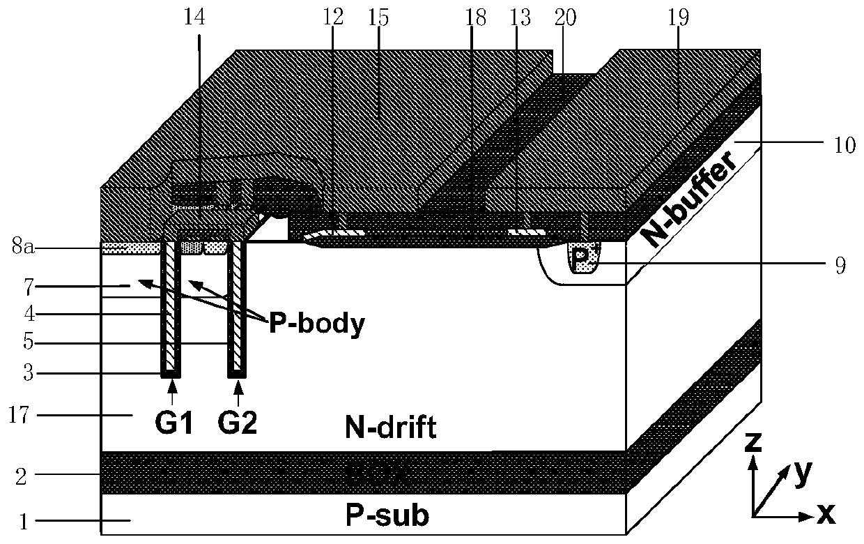
[0029] A trench gate type silicon-on-insulator lateral insulated gate bipolar transistor device, comprising: a P-type substrate 1, a buried oxygen 2 is arranged on the P-type substrate 1, and an N-type drift region is arranged on the buried oxygen 2 17. An N-type buffer zone 10 and a P-type body region 7 are respectively arranged on both sides of the N-type drift region 17, and a heavily doped P-type collector region 9 is arranged in the N-type buffer region 10, and the N-type drift zone A field oxygen layer 18 is provided above the region 17, and one side boundary of the field oxygen layer 18 falls above the N-type buffer zone 10, and the other side boundary is between the P-type body region 7 and the N-type buffer zone 10. Above the N-type drift region 17, a collector polysilicon field plate (13) is provided on the field oxygen layer 18, and the collector...


PUM

PropertyMeasurementUnit
depthaaaaaaaaaa
depthaaaaaaaaaa

Abstract

The invention discloses a trench gate type silicon-on-insulator transverse insulated gate bipolar transistor device. According to the device of the invention, buried oxide is arranged on a P-type substrate; an N-type drift region is arranged on the buried oxide; a P-type body region and an N-type buffer region are arranged on the N-type drift region; a P-type collector region is arranged in the N-type buffer region; a square-wave-shaped heavily-doped N-type emitter region and a square-wave-shaped heavily-doped P-type emitter region are arranged in the P-type body region side by side; and a first square-wave-shaped longitudinal trench and a second square-wave-shaped longitudinal trench are formed on two sides of the square-wave-shaped heavily-doped N-type emitter region and the square-wave-shaped heavily-doped P-type emitter region; the first longitudinal trench is provided with a first polycrystalline silicon layer wrapped by a voltage-withstanding medium; a portion of the second longitudinal trench, which is parallel to the heavily doped P-type collector region, is filled with a second polycrystalline silicon layer wrapped by a voltage-withstanding medium; and a portion of the second longitudinal trench, which is located in a direction from the heavily-doped N-type emitter region to the heavily-doped P-type collector region, is filled with a third polycrystalline silicon layerand an oxide block body, wherein the third polycrystalline silicon layer is wrapped by a voltage-withstanding medium, and the oxide block body is positioned above the third polycrystalline silicon layer; and the second polycrystalline silicon layer is connected with the third polycrystalline silicon layer.

Description

technical field [0001] The present invention mainly relates to the technical field of power semiconductor structures, specifically, it is especially suitable for high-power integrated circuits such as frequency conversion speed regulation, high-voltage power transmission, electric traction, frequency conversion household appliances, half-bridge drive circuits, and automobile production. Background technique [0002] Insulated gate bipolar transistor is a composite power structure evolved from the combination of MOS gate structure and bipolar transistor structure. It perfectly combines the advantages of fast switching speed of MOS tube and strong current capacity of bipolar transistor, and has been widely used. It is widely used in frequency conversion household appliances, induction heating, industrial frequency conversion, photovoltaic power generation, wind power generation, locomotive traction and other fields. Among them, the silicon-on-insulator lateral insulated gate b...

Claims


Application Information

Patent Timeline
Patent Type & Authority Applications(China)
IPC IPC(8): H01L29/06H01L29/423H01L29/739
CPCH01L29/7393H01L29/0615H01L29/0688H01L29/42356Y02B70/10
Inventor 张龙曹梦玲祝靖孙伟锋陆生礼时龙兴
Owner SOUTHEAST UNIV
Why Eureka
Try Eureka