Power source management architecture and boost converter applied to power source management architecture

A boost converter and power management technology, which is applied in the field of boost converters, can solve problems such as large output ripple, low power supply efficiency in the step-down link, and deterioration of efficiency, and achieve wide input and output ranges, reduce overall machine costs, Effect of improving power supply efficiency

Active Publication Date: 2020-01-24
XI AN JIAOTONG UNIV
View PDF2 Cites 0 Cited by
  • Summary
  • Abstract
  • Description
  • Claims
  • Application Information

AI Technical Summary

Problems solved by technology

Traditional power management uses a step-down DC-DC converter to step down the input voltage and then supply power to the digital circuit through the LDO. As the scale of the digital circuit in the SoC increases, more and more energy is consumed in the link where the LDO supplies power to the digital circuit. The power supply efficiency of the entire power management module is reduced
As the operating voltage of digital circuits continues to decrease and the current continues to increase, the overall efficiency of traditional solutions will further deteriorate
[0003] The power management module in the SoC has the problem that the power supply efficiency of the step-down link is low due to the power supply requirements of the digital circuit, and the proportion of the digital circuit in the future SoC will further increase, which will make the efficiency continue to deteriorate.
The traditional Boost structure has a right-half-plane zero point, which requires complex loop compensation in the design. At the same time, the large output ripple makes designers reluctant to choose the Boost structure to avoid performance degradation of noise-sensitive circuits in SoCs.
Switched capacitors can only produce a fixed output voltage due to their structure, which is not suitable for SoC applications

Method used


Image

  • Power source management architecture and boost converter applied to power source management architecture
  • Power source management architecture and boost converter applied to power source management architecture
  • Power source management architecture and boost converter applied to power source management architecture

Examples


Embodiment Construction

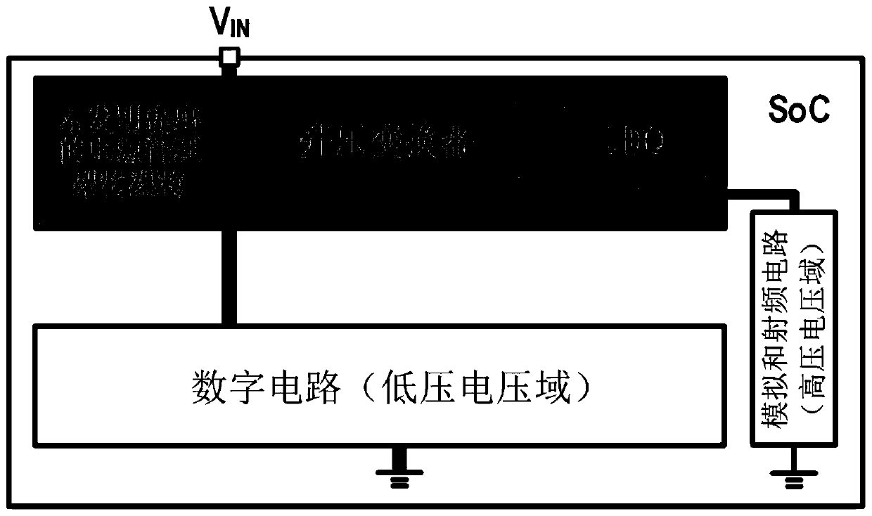
[0033] The present invention provides a power management architecture. The SoC external power supply directly provides low voltage for digital circuit power supply. The internal power management module uses a boost converter to convert the low voltage to high voltage to supply power for the required analog and radio frequency circuits. Improve the power supply efficiency of the SoC power management module.

[0034] see figure 1 , a power management architecture of the present invention can constitute a power management module inside the SoC, and can also appear in the form of a power management chip outside the SoC. The pin V that provides a low voltage power supply for digital circuits IN It is directly connected to the digital circuit in the SoC system level chip, and connected to the input terminal of the boost converter. The output terminal of the boost converter is connected to the power supply of the low dropout linear regulator LDO, and the low dropout linear regulator...


PUM


Abstract

The invention discloses a power source management architecture and a boost converter applied to the power source management architecture. The power source management architecture comprises a boost converter; the input end of the boost converter is connected with a pin VIN and a digital circuit, wherein the pin VIN is used for providing a low-voltage power source for the digital circuit, and the digital circuit is located in an SoC (system-in-chip); the output end of the boost converter is connected with the power source of a low-dropout output linear voltage regulator (LDO); and the output ofthe low-dropout output linear voltage regulator (LDO) provides a high-voltage power source for analog and radio frequency circuits. The boost converter has the advantages of high efficiency, low ripple and wide input and output range. With the power source management architecture adopted, overall power supply efficiency is improved. The power source management architecture is suitable for SoC power supply solutions under advanced processes.

Description

technical field [0001] The invention belongs to the technical field of design of semiconductor integrated circuits and power electronic systems, and in particular relates to a power management architecture and a boost converter applied to the power management architecture. Background technique [0002] The power management module is widely used in electronic equipment to realize the modulation of the power supply, so as to meet the demand of the load for the power supply. For a system on chip (System on Chip, SoC), the power management module converts the off-chip voltage to a lower voltage through a step-down converter for use by digital circuits, analog circuits and radio frequency circuits in the SoC. The current ratio of the digital circuit and the analog circuit integrated in the SoC can reach 10:1 or even higher. At the same time, since digital circuits can well match the process of scaling down, more and more analog and RF modules in SoC are implemented by digital ci...

Claims


Application Information

Patent Timeline
Patent Type & Authority Applications(China)
IPC IPC(8): H02M3/07H02M1/14
CPCH02M1/14H02M3/073H02M1/0012
Inventor 耿莉郭卓奇薛仲明董力
Owner XI AN JIAOTONG UNIV
Why Eureka
Try Eureka