Composite metal oxide semiconductor, thin-film transistor and application

A technology of oxide semiconductors and thin film transistors, which is applied in the manufacture of transistors, semiconductor devices, semiconductor/solid-state devices, etc., can solve problems such as poor light stability, and achieve the effects of improving stability, increasing the degree of overlap, and reducing doping concentration

Pending Publication Date: 2020-02-07
SOUTH CHINA UNIV OF TECH
View PDF9 Cites 11 Cited by
  • Summary
  • Abstract
  • Description
  • Claims
  • Application Information

AI Technical Summary

Problems solved by technology

These photogenerated holes are easily injected into the gate insulating layer under the action of an electric field, which leads to the problem of poor photostability in conventional oxide semiconductors.

Method used


Image

  • Composite metal oxide semiconductor, thin-film transistor and application
  • Composite metal oxide semiconductor, thin-film transistor and application
  • Composite metal oxide semiconductor, thin-film transistor and application

Examples


Embodiment 1

[0046] Example 1: Ytterbium Oxide Doped Indium Gallium Oxide Semiconductor Material

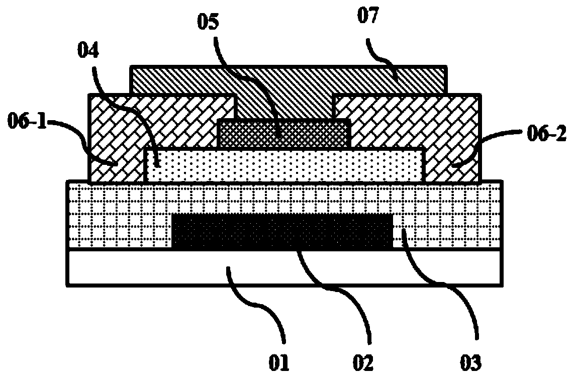
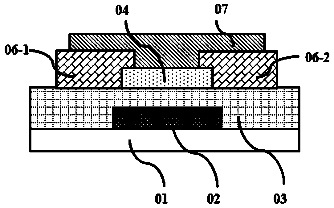
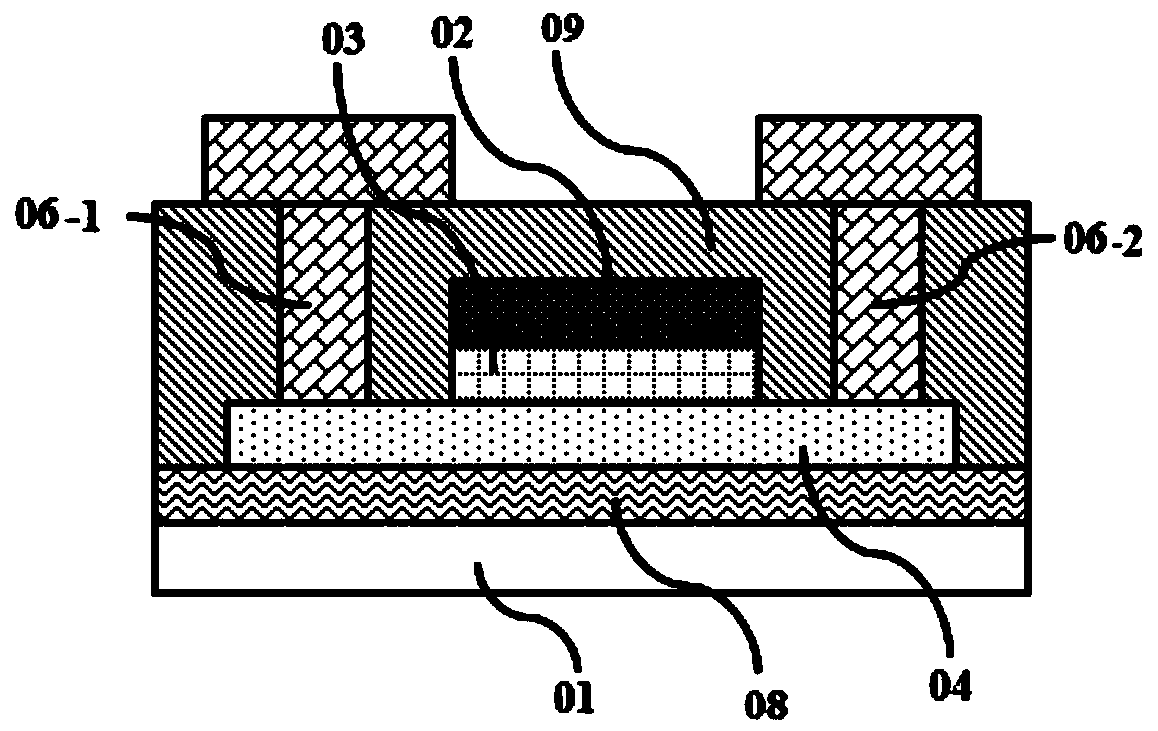
[0047] A group of metal oxide semiconductor materials, the group of metal oxide semiconductor materials are: doping ytterbium oxide in indium gallium oxide (IGO) as a light stabilizer to form a semiconductor material of ytterbium oxide doped indium gallium oxide (Yb:IGO) .

[0048] Among them, in indium gallium oxide, the molar ratio of In and Ga is In:Ga=5:4; in ytterbium oxide doped indium gallium oxide, the molar ratio of ytterbium to indium gallium oxide is 0.002, 0.020, 0.100, 0.200, 0.40 and 0.60.

Embodiment 2

[0049] Example 2: Ytterbium Oxide Doped Indium Zinc Oxide Semiconductor Material

[0050] A group of metal oxide semiconductor materials, the group of metal oxide semiconductor materials are: doping ytterbium oxide in indium zinc oxide (IZO) as a light stabilizer to form a semiconductor material of ytterbium oxide doped indium zinc oxide (Yb:IZO) .

[0051] In indium zinc oxide, the molar ratio of In and Zn is In:Zn=5:1; in ytterbium oxide doped indium zinc oxide, the molar ratios of ytterbium and indium zinc oxide are 0.002, 0.020, 0.100, 0.200, 0.40, respectively and 0.60.

Embodiment 3

[0052] Embodiment 3: Praseodymium oxide doped indium gallium zinc oxide semiconductor material

[0053] A metal oxide semiconductor material, the metal oxide semiconductor material is: indium gallium zinc oxide (IGZO) is doped with praseodymium oxide as a light stabilizer to form a semiconductor of praseodymium oxide doped indium gallium zinc oxide (Pr:IGZO) Material.

[0054] In indium gallium zinc oxide, the molar ratio of In, Ga, and Zn is In:Ga:Zn=3.170:1.585:1; in praseodymium oxide doped indium gallium zinc oxide, the molar ratios of praseodymium and indium gallium zinc oxide are respectively 0.002, 0.020, 0.100, 0.200, 0.40, and 0.60.


PUM

PropertyMeasurementUnit
thicknessaaaaaaaaaa
thicknessaaaaaaaaaa
thicknessaaaaaaaaaa

Abstract

The invention discloses a composite metal oxide semiconductor. The composite metal oxide semiconductor is formed by doping rare earth oxide in metal oxide, wherein the composite metal oxide can effectively inhibit the concentration of oxygen vacancy in a thin-film under the lower doping concentration of ytterbium oxide or praseodymium oxide, and meanwhile, the mobility of the composite metal oxidesemiconductor can be kept at a higher value; the key is that the formed film can avoid the influence on I-V characteristics and stability by illumination, and the stability of the metal oxide semiconductor device under illumination can be greatly improved. The invention also provides a thin-film transistor based on the composite metal oxide semiconductor and an application thereof.

Description

technical field [0001] The invention relates to the field of semiconductor manufacturing, in particular to materials and device structures used in the manufacture of metal oxide semiconductor thin film transistor backplanes in flat panel display and detector applications, and in particular to compound metal oxide semiconductors and thin film transistors and their applications. Background technique [0002] For existing metal oxide semiconductor systems, In 3+ The 5s orbital of the ion is the main electron transport channel. However, due to the low bond breaking energy after In ions form bonds with O ions, in pure In 2 o 3 There are a large number of oxygen vacancy defects in the film. Oxygen vacancies are the main reason for the deterioration of the stability of metal oxide thin film transistors. Usually, doping with In 3+ Ga 3+ Ions regulate the oxygen vacancies. [0003] At the same time, in order to ensure the performance uniformity of the semiconductor device, the...

Claims


Application Information

Patent Timeline
Patent Type & Authority Applications(China)
IPC IPC(8): H01L29/24H01L29/786H01L21/34H01L27/12
CPCH01L29/247H01L29/78693H01L29/66969H01L27/1225H01L29/6675
Inventor 徐苗徐华吴为敬陈为峰王磊彭俊彪
Owner SOUTH CHINA UNIV OF TECH
Why Eureka
Try Eureka