Electroplating method and system of light-emitting diode support and light-emitting diode support
A technology of light-emitting diodes and electroplating nickel, which is applied in the direction of electrolytic process and electrolytic components, can solve the problems of reduced product quality, low thickness coating binding force, poor effect, etc., and achieve the effect of enhancing binding force and improving product quality
- Summary
- Abstract
- Description
- Claims
- Application Information
AI Technical Summary
Problems solved by technology
Method used
Image

Examples
no. 1 example
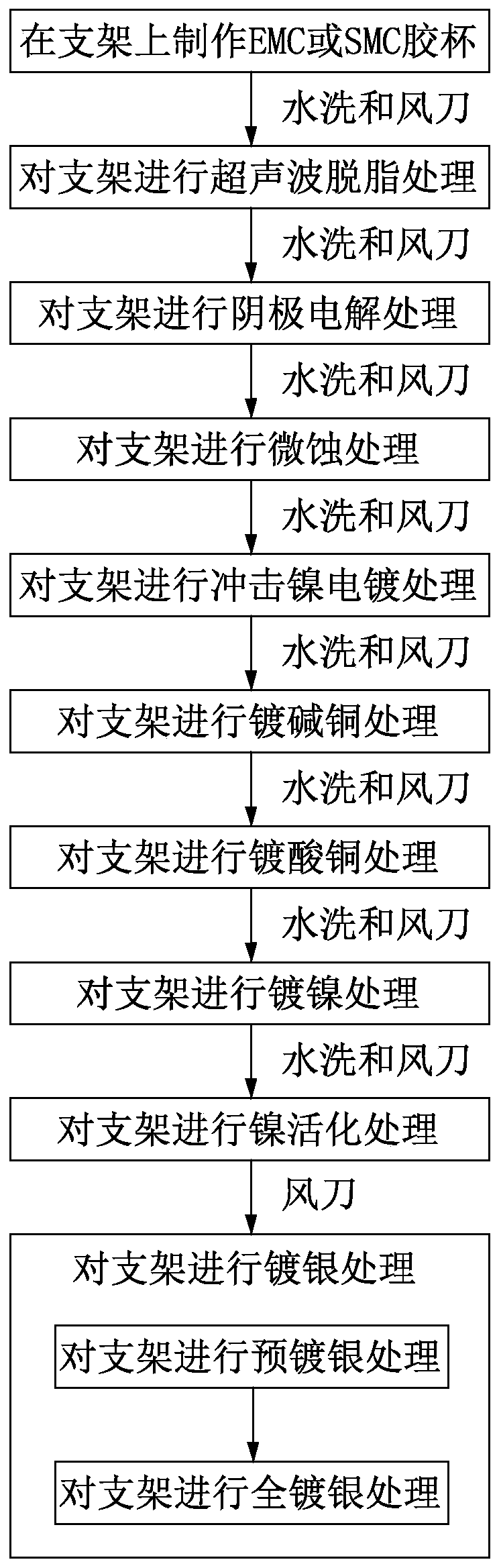
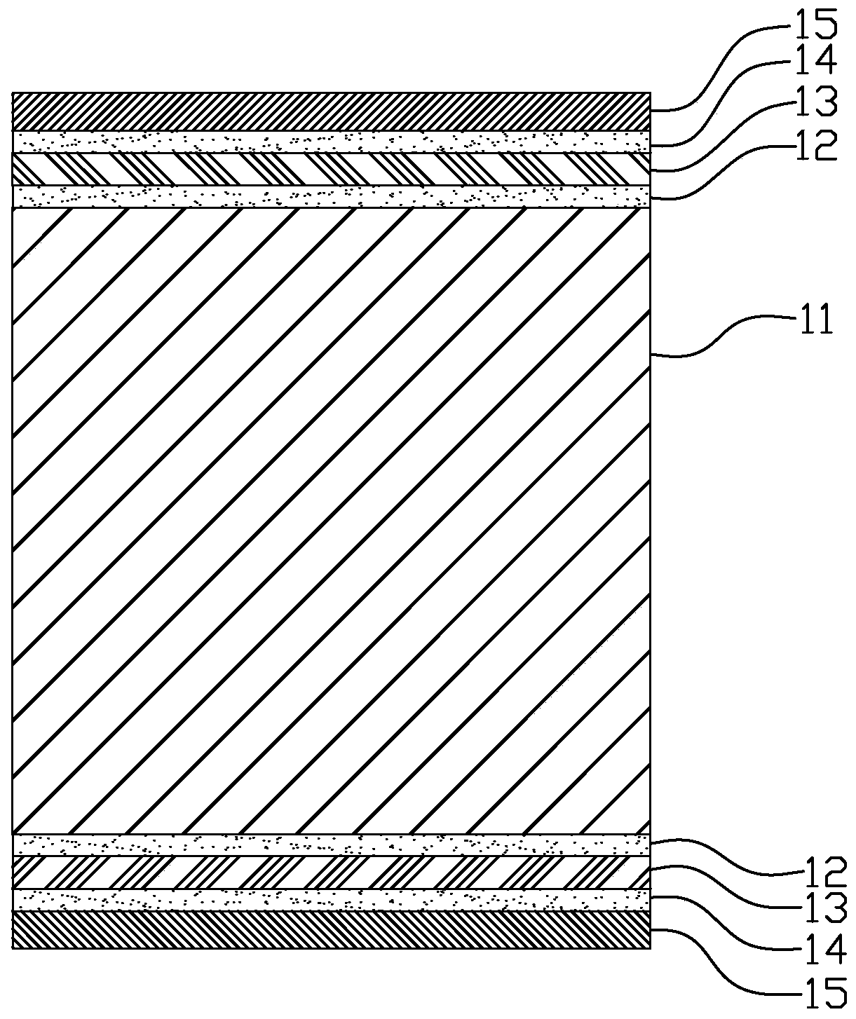
[0057] figure 1 It is a schematic flow chart of the electroplating method of the LED bracket according to the first embodiment of the present invention, figure 2 It is a schematic cross-sectional view of the bracket after electroplating by the electroplating method of the light-emitting diode bracket according to the first embodiment of the present invention, as figure 1 and figure 2 As shown, the electroplating method of the light-emitting diode bracket includes:
[0058] Carry out micro-etching treatment to support 11, remove the oxide layer on the surface of support 11 and activate the surface of support 11; layer or impurities and activate the surface of the stent 11, and at the same time neutralize the alkaline film remaining on the surface of the stent 11, which is conducive to improving the bonding force between the subsequent metal plating layer and the stent 11.
[0059] Further, the parameters for the microetching treatment on the bracket 11 are:
[0060] Sulfuri...
no. 2 example
[0102] The present invention also relates to a light-emitting diode bracket 11, which is formed by using the electroplating method for the above-mentioned light-emitting diode bracket.
[0103] Such as figure 2 As shown, the body surface of the bracket 11 is covered with the first electroplated nickel layer 12, and the bonding force between the first electroplated nickel layer 12 and the electroplated copper layer 13 is strong, so after the treatment of alkali copper plating and acid copper plating, the electroplated copper layer 13 can be firm Groundly combined on the first electroplated nickel layer 12, it is beneficial to strengthen the binding force of the subsequent plating layer, and then improve product quality, the second electroplated nickel layer 14 is formed on the electroplated copper layer 13, the second electroplated nickel layer 14 and the electroplated copper layer 13 1. The binding force of the electroplated silver layer 15 is strong, so after the pre-silveri...
no. 3 example
[0105] The present invention also relates to an electroplating system for a light-emitting diode bracket, which adopts the above-mentioned electroplating method for a light-emitting diode bracket.
[0106] Figure 4 It is a structural schematic diagram of the electroplating system of the light-emitting diode bracket of the third embodiment of the present invention, as figure 1 , figure 2 and Figure 4 As shown, the electroplating system of LED support 11 comprises: feeding device 22, receiving device 33 and the microetching device 25 that is arranged between feeding device 22 and receiving device 33 successively, impact nickel electroplating device 26, alkali plating Copper device 27, nickel electroplating device 29 and silver plating device 32, wherein:
[0107] The bracket 11 output by the feeding device 22 passes through the micro-etching device 25, the impact nickel electroplating device 26, the alkali copper plating device 27, the electro-nickel plating device 29 and ...
PUM
| Property | Measurement | Unit |
|---|---|---|
| thickness | aaaaa | aaaaa |
| thickness | aaaaa | aaaaa |
| thickness | aaaaa | aaaaa |
Abstract
Description
Claims
Application Information
 - R&D
- Intellectual Property
- Life Sciences
- Materials
- Tech Scout
- Unparalleled Data Quality
- Higher Quality Content
- 60% Fewer Hallucinations
Browse by: Latest US Patents, China's latest patents, Technical Efficacy Thesaurus, Application Domain, Technology Topic, Popular Technical Reports.
© 2025 PatSnap. All rights reserved.Legal|Privacy policy|Modern Slavery Act Transparency Statement|Sitemap|About US| Contact US: help@patsnap.com