High-efficiency laser direct-writing photoetching method capable of realizing long-focal-depth small-focal-spot structure

A laser direct writing, high-efficiency technology, used in microlithography exposure equipment, optics, opto-mechanical equipment, etc. The effect of deep and long, small focal spot, improving work efficiency

Active Publication Date: 2020-02-25
INST OF OPTICS & ELECTRONICS - CHINESE ACAD OF SCI
View PDF7 Cites 2 Cited by
  • Summary
  • Abstract
  • Description
  • Claims
  • Application Information

AI Technical Summary

Problems solved by technology

Improving the resolution and depth of focus of the laser direct writing lithography system has always been the focus of research by researchers. The traditional method to improve the lithography resolution is to shorten the exposure wavelength and increase the numerical aperture of the lithography objective lens, but this method is improving resolution while sharply reducing the depth of focus
In addition, traditional laser direct writing lithography requires the use of a translation stage to achieve mechanical scanning, but the precision of mechanical line displacement is related to the size of the range of motion. The larger the displacement range, the lower the positioning accuracy. In precision laser direct writing equipment , requiring high-speed, high-precision positioning and linkage, but high-speed, large-range motion and high-precision, high-resolution mutual constraints

Method used


Image

  • High-efficiency laser direct-writing photoetching method capable of realizing long-focal-depth small-focal-spot structure
  • High-efficiency laser direct-writing photoetching method capable of realizing long-focal-depth small-focal-spot structure
  • High-efficiency laser direct-writing photoetching method capable of realizing long-focal-depth small-focal-spot structure

Examples


Embodiment Construction

[0024] In order to better understand the scanning scheme of the present invention, a further detailed description will be made below in conjunction with the accompanying drawings.

[0025] The present invention is a high-efficiency laser direct writing lithography method capable of realizing long focal depth and small focal spot structure, and the specific steps are as follows:

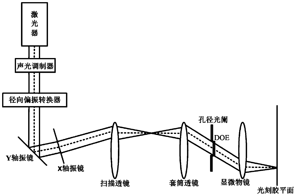
[0026] Step 1: Combine the two-dimensional galvanometer system, scanning lens, tube lens, diaphragm, DOE, and high numerical aperture microscope objective such as figure 1 Adjust to coaxial contour as shown;

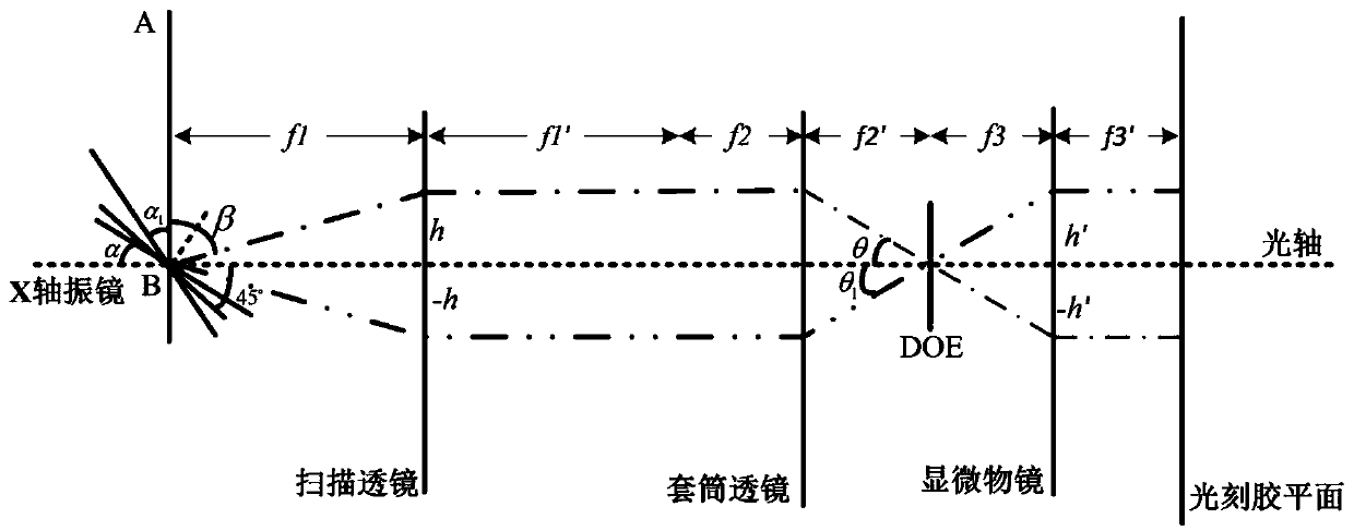
[0027] Step 2: If figure 2 As shown, adjust the center of the X-axis galvanometer of the two-dimensional galvanometer system to coincide with the object focus of the scanning lens, the image focus of the scan lens coincides with the object focus of the sleeve lens, and the image focus of the sleeve lens It is coincident with the focal point of the object side of the high numerical aperture mi...


PUM


Abstract

The invention discloses a high-efficiency laser direct-writing photoetching method capable of realizing a long-focal-depth small-focal-spot structure. Phase modulation is carried out through DOE, so that the diffraction limit can be exceeded, and the resolution and the focal depth of an optical pin are improved; movement of the optical pin on a photoresist plane can be achieved through optical scanning, and the laser direct writing photoetching speed is increased. The optical scanning system utilizes a two-dimensional galvanometer system to generate small-angle deflection of -10 degrees to +10degrees in the X-axis direction and the Y-axis direction. An X-axis galvanometer vibrates along the X-axis direction, a Y-axis galvanometer vibrates along the Y-axis direction, the galvanometers arerespectively driven by two drivers, incident radial polarized light passes through the X-axis galvanometer and the Y-axis galvanometer and then obliquely enters through a scanning lens, a sleeve lens,a pure-phase binary optical element and a high-numerical-aperture microscope objective in sequence, and then an optical pin which moves along the X axis and the Y axis and has resolution, focal depthand uniformity not affected by angle deflection is generated near a focal plane. And the resolution, the focal depth and the direct writing efficiency of laser direct writing photoetching are improved.

Description

technical field [0001] The invention belongs to the field of micro-nano processing, and in particular relates to a high-efficiency laser direct writing photolithography method capable of realizing a long focal depth and small focal spot structure. Background technique [0002] Laser direct writing lithography is one of the main technologies for making diffractive optical elements. Compared with traditional mask lithography, laser direct writing lithography has the advantages of no mask, flexible processing, and low requirements on the flatness of the substrate surface. At present, laser direct writing technology is mainly used in integrated circuit manufacturing, material surface treatment and etching, diffractive optical element processing, micro-nano structure device manufacturing and other fields. Improving the resolution and depth of focus of the laser direct writing lithography system has always been the focus of research by researchers. The traditional method to improv...

Claims


Application Information

Patent Timeline
Patent Type & Authority Applications(China)
IPC IPC(8): G03F7/20
CPCG03F7/2051G03F7/70316G03F7/70358
Inventor 王思沫严伟史立芳李凡星彭伏平杜佳林
Owner INST OF OPTICS & ELECTRONICS - CHINESE ACAD OF SCI
Why Eureka
Try Eureka