TO tube socket packaging structure and manufacturing method thereof

A technology of packaging structure and manufacturing method, which is applied in the direction of laser parts, electrical components, lasers, etc., can solve the problems of limiting the technical level and application range of TO tube sockets, mismatching of different materials welding, and inability to maintain positional accuracy, etc., to avoid Product surface defects and repeated processing, high installation efficiency, and improved electro-optical conversion efficiency

Pending Publication Date: 2020-02-28
WUHAN UNICELL TECH CO LTD
View PDF0 Cites 2 Cited by
  • Summary
  • Abstract
  • Description
  • Claims
  • Application Information

AI Technical Summary

Problems solved by technology

The laser chip installed inside the TO tube socket and the structures such as lenses have extremely high precision requirements, but in actual use, the laser chip will generate a lot of heat, due to the different thermal expansion coefficients of the materials in the TO tube socket , will cause the original position accuracy to be unable to be maintained. At the same time, the internal tightness of the TO tube socket is required to be high. Generally, welding is used for sealing, but the heat generated during the welding process will also cause thermal deformation of the material to varying degrees. , so there will be a mismatch when welding different materials, and the welding process requirements are very high. The above-mentioned problems make it difficult to achieve a good coordination between the accuracy, life and cost of the existing TO tube socket products, which limits the TO tube socket technical level and scope of application

Method used


Image

  • TO tube socket packaging structure and manufacturing method thereof
  • TO tube socket packaging structure and manufacturing method thereof
  • TO tube socket packaging structure and manufacturing method thereof

Examples


Embodiment Construction

[0026] The invention will be described in detail below in conjunction with specific embodiments.

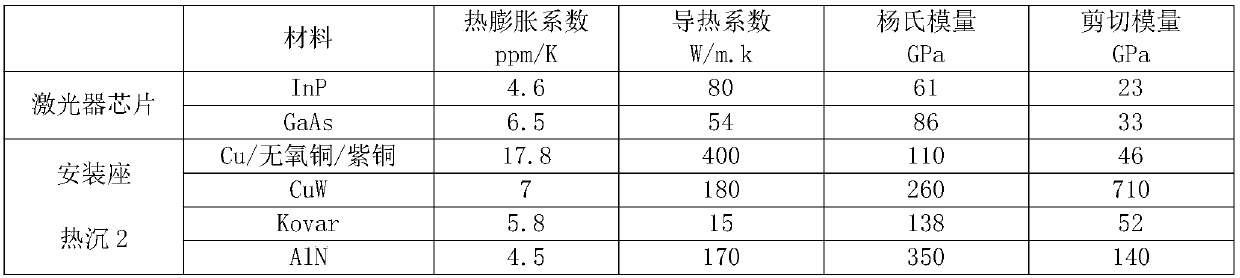
[0027] The invention relates to a packaging structure of a TO tube base. The TO tube is the basic hardware of various lasers, and is the basis for ensuring the continuous and stable operation of the lasers and completing various photoelectric conversions. Several types of materials commonly used in the laser industry include several in Table 1 below;

[0028] Table 1 Properties of materials commonly used in lasers

[0029]

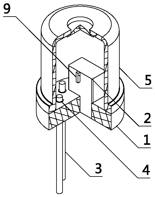
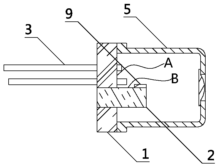
[0030] Usually, the TO socket is composed of a mounting seat for supporting the overall structure and connecting leads and other structures, and a heat sink 2 fixedly arranged on the mounting seat. The sink 2 is used to install the laser chip 9; as can be seen from Table 1, in order to improve the accuracy of the laser, the heat sink 2 is generally made of Kovar alloy, copper and tungsten copper, but the thermal conductivity of the Kovar alloy is poor, so...


PUM


Abstract

The invention belongs to the technical field of optical communication device designing and manufacturing, and particularly relates to a TO tube socket packaging structure and a manufacturing method thereof. The TO tube socket packaging structure comprises a TO tube socket, and the TO tube socket comprises a mounting base made of a kovar alloy material and a heat sink arranged on the mounting base.A plurality of lead holes are formed in the mounting base, and leads are arranged in the lead holes respectively. A mounting hole is further formed in the mounting base, the mounting hole penetratesthrough the mounting base, and the heat sink is inserted into the mounting hole and connected in a sealed mode through silver-copper brazing. The invention further relates to a manufacturing method ofthe TO tube socket packaging structure, which comprises the following steps: machining a mounting base 1; welding leads 3; and machining a heat sink 2. The TO tube socket structure has high heat efficiency, long service life and high electro-optical conversion efficiency. The structure and the manufacturing method of the invention have the characteristics of easy-to-guarantee positioning precision, high mounting efficiency and the like. The structure is simplified, the production difficulty and cost are reduced, and the product performance is improved.

Description

technical field [0001] The invention belongs to the technical field of optical communication device design and manufacture, and in particular relates to a TO socket packaging structure and a manufacturing method thereof. Background technique [0002] The TO package consists of two components: a base and a cap. The stem ensures that the electrical signal is supplied to the packaged components, while the cap ensures the smooth transmission of the optical signal. The TO socket (also known as the base) provides a mechanical basis for mounting electronic and optical components such as semiconductors, laser diodes or simple circuits, while providing electrical signals to packaged components through leads. In optoelectronic applications, TO headers can be used in all conventional applications (also on the transmitter side (TOSA) and receiver side (ROSA) of transceivers), as well as high-speed data transmission, infrared applications, etc. The laser chip installed inside the TO tu...

Claims


Application Information

Patent Timeline
Patent Type & Authority Applications(China)
IPC IPC(8): H01S5/022H01S5/024
CPCH01S5/02469H01S5/0231H01S5/02325H01S5/02345
Inventor 苗祺壮方俊
Owner WUHAN UNICELL TECH CO LTD
Why Eureka
Try Eureka