
5G high-frequency circuit board solder mask pretreatment method

A high-frequency circuit board and circuit board technology, which is applied in the secondary processing of printed circuits, printed circuits, and printed circuit manufacturing, can solve the problem of poor bonding between high-frequency circuit board substrates and silk screen inks, and reduce high-frequency circuit board processing. Efficiency, prone to oil throwing and other problems, to avoid surface oxidation, increase contact surface, good effect

Inactive Publication Date: 2020-02-28
SHANGHAI SECOND POLYTECHNIC UNIVERSITY
View PDF7 Cites 5 Cited by
  • Summary
  • Abstract
  • Description
  • Claims
  • Application Information

AI Technical Summary

Problems solved by technology

[0004] Aiming at the deficiencies of the prior art, the present invention provides a pre-treatment method for 5G high-frequency circuit board solder resistance, which solves the problem of poor bonding between the base material of the high-frequency circuit board and the screen printing ink, which is prone to oil rejection, and high Ink bubbles are prone to appear on the substrate of high-frequency circuit boards, which reduces the processing efficiency of high-frequency circuit boards

Method used


Image

  • 5G high-frequency circuit board solder mask pretreatment method

Examples


Embodiment Construction

[0024] The following will clearly and completely describe the technical solutions in the embodiments of the present invention with reference to the accompanying drawings in the embodiments of the present invention. Obviously, the described embodiments are only some, not all, embodiments of the present invention. Based on the embodiments of the present invention, all other embodiments obtained by persons of ordinary skill in the art without making creative efforts belong to the protection scope of the present invention.

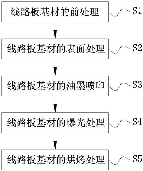
[0025] see figure 1 , the embodiment of the present invention provides a technical solution: a 5G high-frequency circuit board pre-treatment method for solder resistance, which specifically includes the following steps:

[0026] S1. Pretreatment of circuit board base material: place the base material on a grinding machine for grinding treatment, and use pure water to clean the surface of the base material twice after the grinding process is completed, and rins...


PUM

PropertyMeasurementUnit
thicknessaaaaaaaaaa

Abstract

The invention discloses a 5G high-frequency circuit board solder mask pretreatment method, which specifically comprises the following step: S1, a circuit board substrate is pretreated, specifically, the substrate is placed on a board grinding machine to be subjected to board grinding treatment, and the surface of the substrate is cleaned twice with pure water after board grinding treatment of thesubstrate. The invention relates to the technical field of high-frequency circuit board solder mask pretreatment. According to the 5G high-frequency circuit board solder mask pretreatment method, thesubstrate is placed on the board grinding machine to be subjected to board grinding treatment, the surface of the substrate is cleaned twice with pure water after board grinding treatment of the substrate, impurities on the surface of the substrate are washed away, and the circuit board substrate is dried by strong wind, wherein the grinding marks are controlled to be 10-15mm, the linear speed ofa brush plate is 10.8m / s, and a brush roller adopts a large dragging shaft. The contact surface is increased, the ink bubble phenomenon of the circuit board substrate in the ink jet printing process can be avoided, the surface oxidation of the circuit board substrate before solder resisting can be avoided, and the pretreatment effect is good.

Description

technical field [0001] The invention relates to the technical field of pre-treatment of high-frequency circuit boards for solder resistance, in particular to a method for pre-treatment of solder resistance for 5G high-frequency circuit boards. Background technique [0002] The pretreatment steps in the existing high-frequency circuit board solder mask method include: PTFE board pretreatment adopts micro-etching or super-roughening chemical cleaning methods; ceramic boards can use mechanical brushing and chemical cleaning methods, and chemical cleaning is preferred In special cases, mechanical brushing can be used when chemical cleaning is not possible, but the wear marks should be controlled within 0.6-1.0mm, so as to avoid too many board passes and affect the flatness of the copper surface. [0003] 5G high-frequency PTFE board has chemical inertness and low surface energy, and it is difficult to bond with other materials. Among them, sodium etchant will discolor the surfac...

Claims


Application Information

Patent Timeline
Patent Type & Authority Applications(China)
IPC IPC(8): H05K3/28
CPCH05K3/28H05K2203/025H05K2203/0766H05K2203/107H05K2203/11H05K2203/1168H05K2203/1377
Inventor 王德贤汪志锋杨敬辉顾钧杜万和
Owner SHANGHAI SECOND POLYTECHNIC UNIVERSITY
Learn More