Silicon carbide-based reverse switching transistor and preparation method thereof

A reverse switching, silicon carbide-based technology, used in thyristor, semiconductor/solid-state device manufacturing, semiconductor devices, etc., can solve problems such as difficult to precharge plasma layers, and achieve high withstand voltage, simple process, and easy implementation.

Active Publication Date: 2020-03-20
HUAZHONG UNIV OF SCI & TECH
View PDF16 Cites 3 Cited by
  • Summary
  • Abstract
  • Description
  • Claims
  • Application Information

AI Technical Summary

Problems solved by technology

[0007] In view of the above defects or improvement needs of the prior art, the object of the present invention is to provide a silicon carbide-based reverse switching transistor and its preparation method, wherein the detailed structure design of the device and the corresponding preparation method are improved, and the use of N after thinning + type substrate, and inject P at a certain distance from the cathode + Type highly doped ions to form a cathode short circuit point, that is, by pairing N + The type substrate is thinned, and then the N + The cathode region is disconnected, and P is injected at the disconnection + Type highly doped ions to form a cathode short-circuit point, which can realize the effective pre-filling process of RSD, and overcome the inability to well control the defects of the silicon carbide epitaxial wafer in the prior art, which causes the device to be blocked when the avalanche is used to establish the pre-filled plasma layer. Early breakdown, difficult to achieve effective pre-charge plasma layer establishment by utilizing avalanche breakdown

Method used


Image

  • Silicon carbide-based reverse switching transistor and preparation method thereof
  • Silicon carbide-based reverse switching transistor and preparation method thereof
  • Silicon carbide-based reverse switching transistor and preparation method thereof

Examples


Embodiment Construction

[0050] In order to make the object, technical solution and advantages of the present invention clearer, the present invention will be further described in detail below in conjunction with the accompanying drawings and embodiments. It should be understood that the specific embodiments described here are only used to explain the present invention, not to limit the present invention. In addition, the technical features involved in the various embodiments of the present invention described below can be combined with each other as long as they do not constitute a conflict with each other.

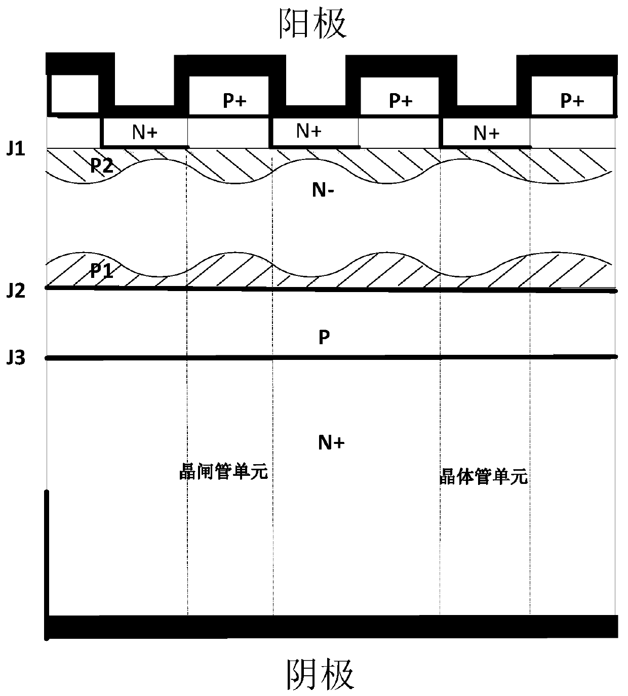
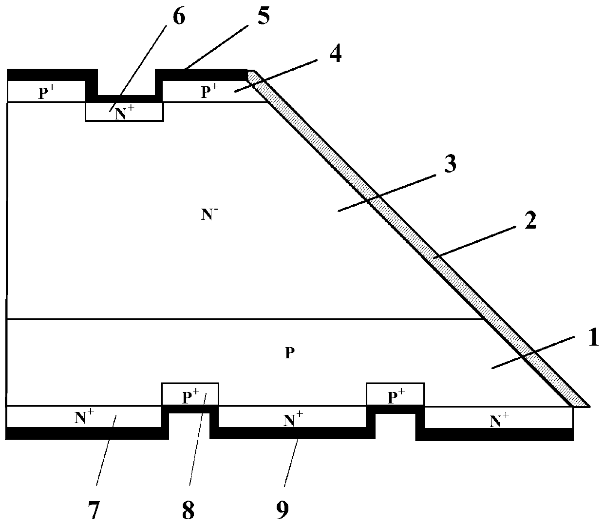
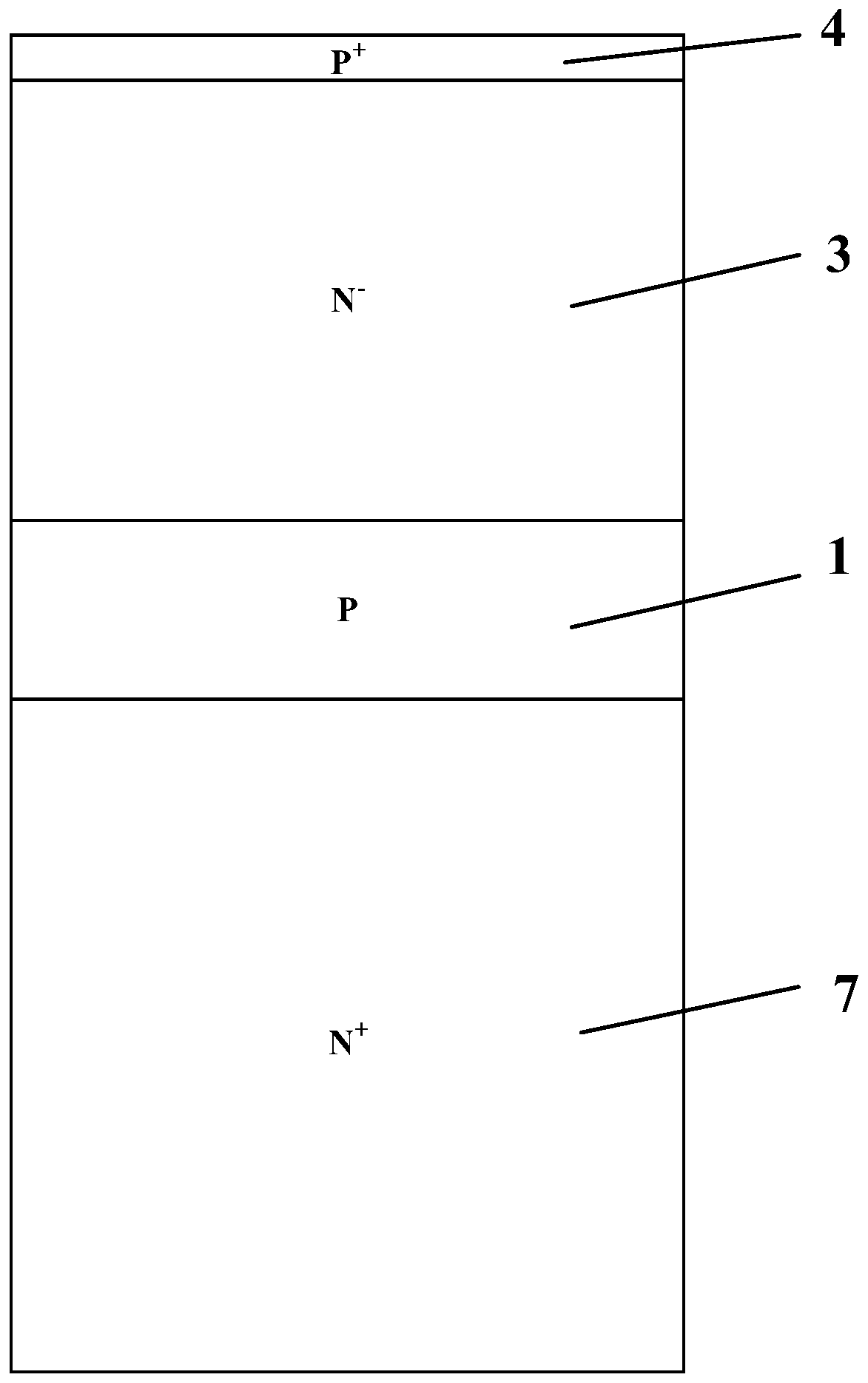
[0051] In the present invention, the reverse switching transistor based on silicon carbide is composed of four layers of PNPN, and the anode is made of P + N + alternating cells. Such as figure 2 shown, including SiC N + Type substrate (7), cathode silicon carbide P + Short circuit (8), silicon carbide P base (1), silicon carbide N - Drift region (3), the anode is made of silicon carbide ...


PUM

PropertyMeasurementUnit
thicknessaaaaaaaaaa
thicknessaaaaaaaaaa
lengthaaaaaaaaaa

Abstract

The invention belongs to the technical field of pulse power devices, and discloses a silicon carbide-based reverse switching transistor and a preparation method thereof, the transistor comprises a silicon carbide N + type substrate (7), a silicon carbide P base region (1), a silicon carbide N-drift region (3) and an anode emitter region from bottom to top; the device adopts a positive bevel angleterminal; the device can conduct current through a cathode short circuit point, namely a silicon carbide cathode P + region (8). According to the invention, the structure and the preparation method ofthe SiC RSD are improved; thinning the N + type substrate; periodically disconnecting the N + cathode region; injecting P + type highly-doped ions into the disconnected part to form a cathode short-circuit point. Therefore, the effective pre-charging process of the RSD is realized, and the problems that the device is broken down in advance when a pre-charging plasma layer is established by utilizing avalanche and the effective pre-charging plasma layer is difficult to establish by utilizing avalanche breakdown due to the fact that the defects of the silicon carbide epitaxial wafer cannot be well controlled in the prior art are solved.

Description

technical field [0001] The invention belongs to the technical field of pulsed power devices, and more specifically relates to a silicon carbide-based reverse switch transistor and a preparation method thereof, which is a structure and process of a wide bandgap semiconductor device, and the obtained silicon carbide reverse switch Transistors can be used in particular in the field of pulsed power technology. Background technique [0002] Pulse power technology plays a very important role in the fields of national defense and military affairs, and the pulse power switch is the core device of the pulse power system. The reverse switching transistor RSD (Reversely switched dynistor) is a pulsed power semiconductor switching device based on the principle of controllable plasma layer triggering, which can realize uniform and synchronous turn-on across the entire area. Compared with IGBT, SCR, etc., it has better voltage equalization characteristics. , higher withstand voltage and ...

Claims


Application Information

Patent Timeline
Patent Type & Authority Applications(China)
IPC IPC(8): H01L29/06H01L29/74H01L21/332
CPCH01L29/0619H01L29/0684H01L29/66068H01L29/74
Inventor 梁琳颜小雪
Owner HUAZHONG UNIV OF SCI & TECH
Why Eureka
Try Eureka