Graphene enhanced absorption metal micro-nano structure and preparation method thereof
A technology of micro-nano structure and graphene, applied in optical components, optics, instruments, etc., can solve the problems of high experimental precision, complicated preparation process, and low light absorption efficiency, and achieve wide absorption spectrum range, enhanced light absorption, fast response effect
- Summary
- Abstract
- Description
- Claims
- Application Information
AI Technical Summary
Problems solved by technology
Method used
Image

Examples
Embodiment 1
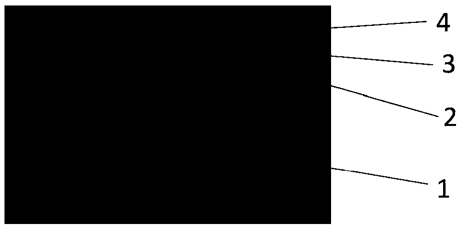
[0044] Such as figure 1 As shown, it is a metal micro-nano structure in this embodiment. The metal micro-nano structure is provided with a first metal layer 2 , a silicon dioxide layer 3 , and a second metal layer 4 on a base layer 1 in sequence.
[0045] Specifically: the base layer 1 is made of silicon or silicon dioxide, the first metal layer 2 and the second metal layer 4 are made of gold or silver, and the embodiment of the present application is preferably silver. Both the thickness of the first metal layer 2 and the second metal layer 4 are 10-50 nm, and the thickness of the silicon dioxide layer 3 is 20-50 nm. In the embodiment of the present application, the thickness of the first metal layer 2 and the thickness of the second metal layer 4 are preferably The thickness of the silicon dioxide layer 3 is 50 nm.
[0046] In the embodiment of the present application, the metal micro-nano structure is composed of the double-layer metal of the first metal layer 2 and the se...
Embodiment 2
[0049]Based on the metal micro-nano structure disclosed in Example 1, the embodiment of the present application also discloses a metal micro-nano structure with graphene-enhanced absorption. Compared with the micro-nano structure disclosed in Example 1, the absorption rate is increased by more than 7%, Moreover, the structure is simple, the preparation is convenient, and the operation is easier.
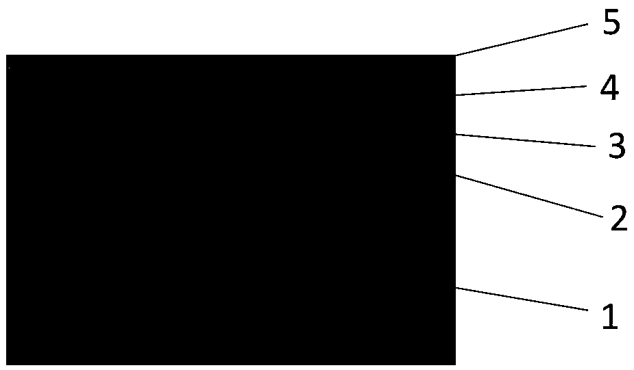
[0050] Such as figure 2 Shown is a metal micro-nano structure with graphene-enhanced absorption in this embodiment. Based on the metal micro-nano structure disclosed in Example 1, the second metal layer 4 is also provided with a first graphene thin film layer 5 .
[0051] Specifically: the first graphene film layer 5 is 1 to 3 layers of graphene, the thickness of the first metal layer 2 is 10 to 50 nm, the thickness of the silicon dioxide layer 3 is 20 to 50 nm, and the thickness of the second metal layer is 20 to 50 nm. The thickness of layer 4 is 10-50 nm. The first metal layer ...
Embodiment 3
[0058] Based on the metal micro-nano structure disclosed in Example 2, the embodiment of the present application also discloses a micro-nano structure. Compared with Example 2, a titanium dioxide film layer is added, and the service life of the metal micro-nano structure is longer.
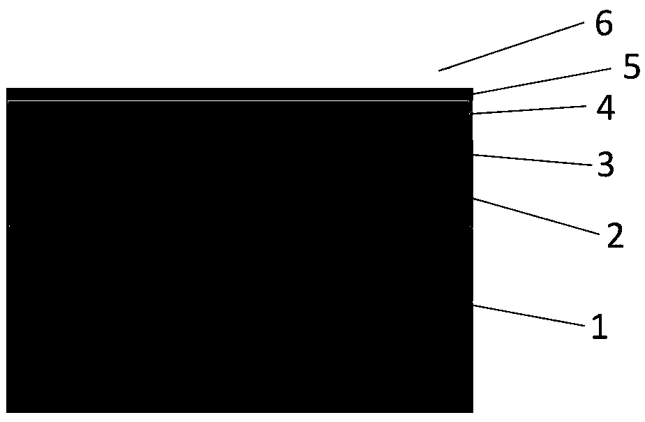
[0059] Such as image 3 Shown is the metal micro-nano structure of the embodiment of the present application. On the basis of embodiment 2, this embodiment also has a titanium dioxide thin film layer 6 on the first graphene thin film layer 5 .
[0060] Specifically: the present embodiment is provided with titanium dioxide layer 6 on the first graphene thin film layer 5, and titanium dioxide can effectively prevent the problem that graphene layer is easy to fall off in preparation and application process, and titanium dioxide will be under the irradiation of ultraviolet light. Generates holes, has strong oxidizing properties, can decompose organic matter and sterilize, and can effectively ensure th...
PUM
| Property | Measurement | Unit |
|---|---|---|
| Thickness | aaaaa | aaaaa |
| Thickness | aaaaa | aaaaa |
| Thickness | aaaaa | aaaaa |
Abstract
Description
Claims
Application Information