Nanoparticle self-assembled transparent circuit board, and preparation method thereof and application thereof

A transparent circuit board and nanoparticle technology, applied in the field of microelectronics, can solve the problems of single production substrate, circuit structure control, cumbersome production steps, etc., and achieve the effect of simple production, low cost and good optical transparency

Active Publication Date: 2020-03-27
HUAZHONG UNIV OF SCI & TECH
View PDF5 Cites 8 Cited by
  • Summary
  • Abstract
  • Description
  • Claims
  • Application Information

AI Technical Summary

Problems solved by technology

[0004] The invention overcomes the shortcomings of the existing circuit manufacturing technology in terms of circuit structure control, cumbersome manufacturing steps, dependence on specific equipment, single manufacturing substrate, etc., and provides a transparent circuit board self-assembled by nanoparticles and a preparation method

Method used


Image

  • Nanoparticle self-assembled transparent circuit board, and preparation method thereof and application thereof
  • Nanoparticle self-assembled transparent circuit board, and preparation method thereof and application thereof
  • Nanoparticle self-assembled transparent circuit board, and preparation method thereof and application thereof

Examples


preparation example Construction

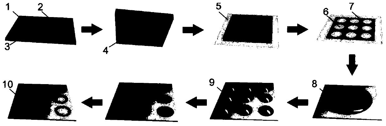
[0041] According to another aspect of the present invention, a method for preparing a nanoparticle self-assembled transparent circuit is provided, comprising the following steps:

[0042] (a) Fabrication of micropatterned PDMS stamps using standard photolithography and rapid imprinting;

[0043] (b) Sandwich the commercial parafilm between the tinfoil and the PDMS stamp obtained in step (a), and place the device with a sandwich structure (the PDMS stamp is on the top layer) on a hot plate and heat at 120°C for 30s;

[0044] (c) tear the PDMS stamp obtained in step (b) off the sealing film, and immediately place it on the target substrate, press the PDMS stamp with your fingers for about 30 seconds at room temperature, and then tear the PDMS stamp off the target substrate;

[0045] (d) adding the water-soluble solution containing nanoparticles to the target substrate obtained in step (c), and using a glass rod to guide the nanoparticle suspension to move over the surface of the t...

Embodiment 1

[0049] A transparent circuit board self-assembled by nanoparticles, the transparent circuit board includes a nanoparticle conductive structure self-assembled based on the coffee ring effect and a hydrophilic transparent substrate; the nanoparticle conductive structure is a hollow structure obtained by self-assembly by the coffee ring effect; The nano particle conductive structure is located on the surface of the hydrophilic transparent substrate; the nano particle conductive structure is distributed in an array.

[0050] The nanoparticles are gold nanoparticles.

[0051] The hydrophilic transparent base is a plastic petri dish; the boundary shape of the hollow structure is a circle.

[0052] The height of the nanoparticle conductive structure is 100 nm, and the boundary width is 1 μm.

[0053] Each conductive nanoparticle structure is located in a square area with a side length of 400 μm, and the distance between centers of gravity of adjacent conductive nanoparticle structur...

Embodiment 2

[0055] A transparent circuit board self-assembled by nanoparticles, the transparent circuit board includes a nanoparticle conductive structure self-assembled based on the coffee ring effect and a hydrophilic transparent substrate; the nanoparticle conductive structure is a hollow structure obtained by self-assembly by the coffee ring effect; The nano particle conductive structure is located on the surface of the hydrophilic transparent substrate; the nano particle conductive structure is distributed in an array.

[0056] The nanoparticles are gold nanoparticles.

[0057] The hydrophilic transparent substrate is glass; the boundary shape of the hollow structure is square.

[0058] The height of the nanoparticle conductive structure is 300 nm, and the boundary width is 3 μm.

[0059] Each of the nanoparticle conductive structures is located in a square area with a side length of 500 μm, and the distance between the centers of gravity of adjacent nanoparticle conductive structur...


PUM

PropertyMeasurementUnit
heightaaaaaaaaaa
widthaaaaaaaaaa
heightaaaaaaaaaa

Abstract

The invention relates to a nanoparticle self-assembled transparent circuit board, a preparation method thereof, and an application thereof, and belongs to the technical field of microelectronics. Thenanoparticle self-assembled transparent circuit board comprises a nanoparticle conductive structure and a hydrophilic transparent substrate, wherein the nanoparticle conductive structure is a hollow structure; the nanoparticle conductive structure is located on the surface of the hydrophilic transparent substrate; and the nanoparticle conductive structures are distributed in an array. The preparation method comprises the following steps: firstly, preparing the hydrophobic seal, paving one side, with the concave part, of the seal on the paraffin film, and heating the paraffin film, so that theparaffin film is converted into a molten state; and setting a seal on a hydrophilic transparent substrate, adhering molten paraffin on the seal to the surface of the hydrophilic transparent substrate,then tearing off the hydrophilic transparent substrate, adding dropwise a nano-particle aqueous solution to the hydrophilic transparent substrate, and forming the transparent circuit board based on nano-particle self-assembly based on the coffee ring effect. The nanoparticle self-assembled transparent circuit board has the advantages of simple and rapid manufacturing, low cost, diversified manufacturing substrates, diversified patterns, high throughput, transparency and the like.

Description

technical field [0001] The invention belongs to the technical field of microelectronics, and relates to a transparent circuit self-assembled by nanoparticles, a preparation method and application thereof. Background technique [0002] Transparent conductive circuits are widely used in displays, light-emitting devices, solar cells, and flexible electronics. Transparent conductive oxides are the most traditional materials used for this purpose, but suffer from limitations such as complex fabrication, expensive, limited supply, and relatively low electrical conductivity. To overcome the above-mentioned problems, a large number of new materials have been developed to obtain transparent conductive circuits, including metal nanoparticles, metal wires, graphene, carbon nanotubes, and conductive polymers. The techniques used to fabricate conductive networks can be divided into two categories: top-down microfabrication techniques and bottom-up self-assembly methods. However, the to...

Claims


Application Information

Patent Timeline
Patent Type & Authority Applications(China)
IPC IPC(8): H01B5/14H01B13/00
CPCH01B5/14H01B13/0026
Inventor 刘笔锋马朋杜伟陈鹏
Owner HUAZHONG UNIV OF SCI & TECH
Why Eureka
Try Eureka