Method for preparing polycrystalline doping molybdenum zinc oxide transparent conductive film
A transparent conductive film, zinc oxide technology, applied in ion implantation plating, metal material coating process, coating and other directions, can solve problems such as high valence state difference, and achieve the effect of good process stability
- Summary
- Abstract
- Description
- Claims
- Application Information
AI Technical Summary
Problems solved by technology
Method used
Image
Examples
Embodiment 1
[0034] Example 1, preparation of zinc-molybdenum metal mosaic target: at a temperature of 450°C, Zn metal with a purity of 99.99% was melted into a target, and molybdenum wire with the same purity of 99.99% was embedded uniformly and symmetrically at 2at%. The target diameter was 60mm and a thickness of 3mm. The substrate is a common glass slide, which has been washed by pure water, alcohol and acetone ultrasonic waves for 15 minutes each.
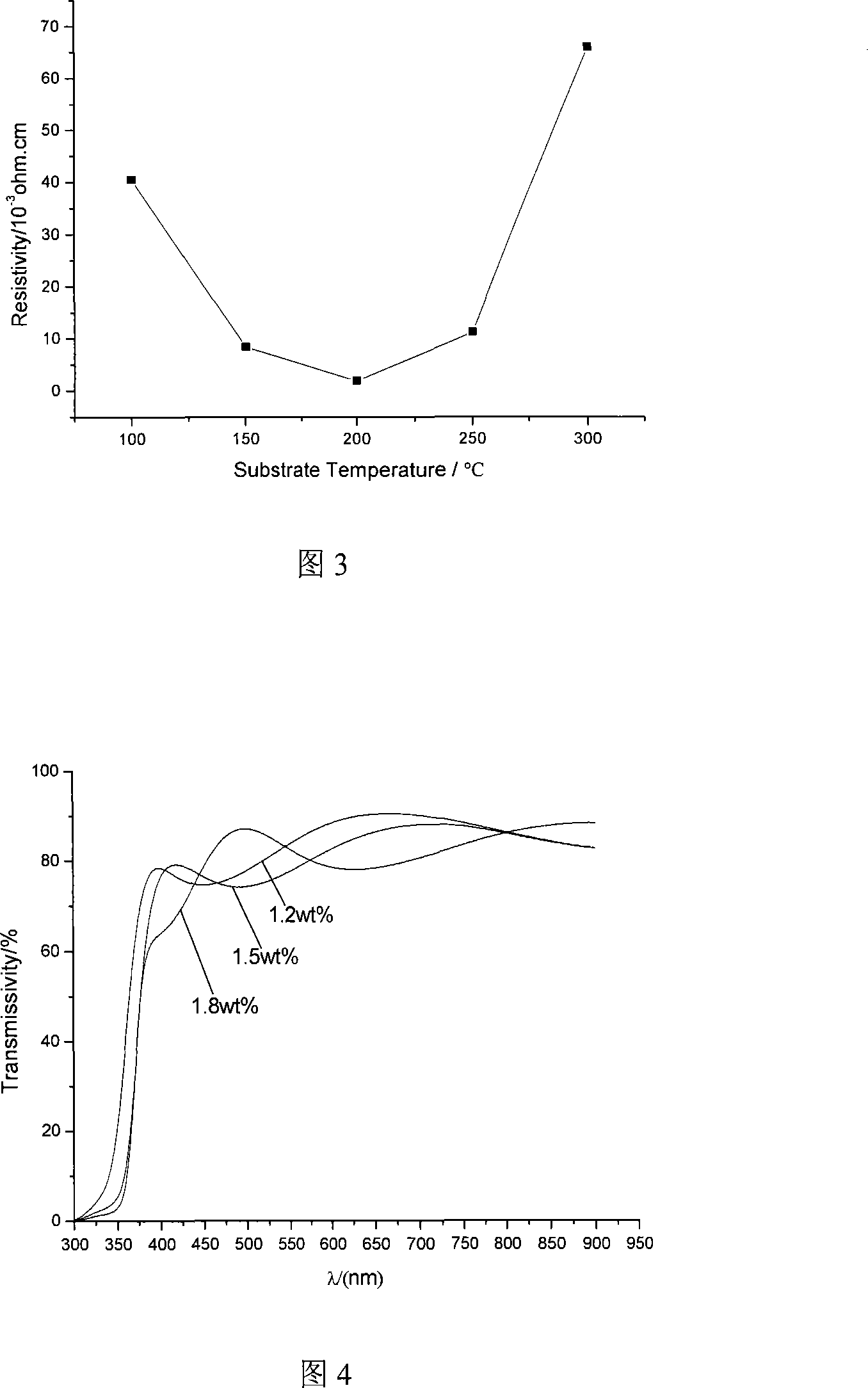
[0035] Substrate temperature: 200°C.
[0036] The distance between the target and the substrate was fixed at 130 mm.
[0037] Before film deposition, the reaction chamber was evacuated to less than 2×10 -3 Pa, then the O through the variable air pilot valve 2 And Ar gas into the reaction chamber. The working pressure in the reaction chamber is 2.5×10 -1 Pa, sputtering current is 200mA, sputtering voltage is 150-160V, control O 2 The percentage of reaction gas 5.0%. The films were prepared on ordinary glass slides.
[0038] Th...
Embodiment 2
[0039] Example 2, at a substrate temperature of 200°C, the same method as in Example 1 was used to prepare a polycrystalline ZMO thin film under the following conditions: the O 2 and Ar gas into the reaction chamber and control the O 2 The percentage of P(O 2 ) is 10%. The sputtering time is 60 minutes, and the film thickness is 150 nm. The resistivity of the prepared ZMO film is 5.54×10 -3 Ω·cm.
Embodiment 3
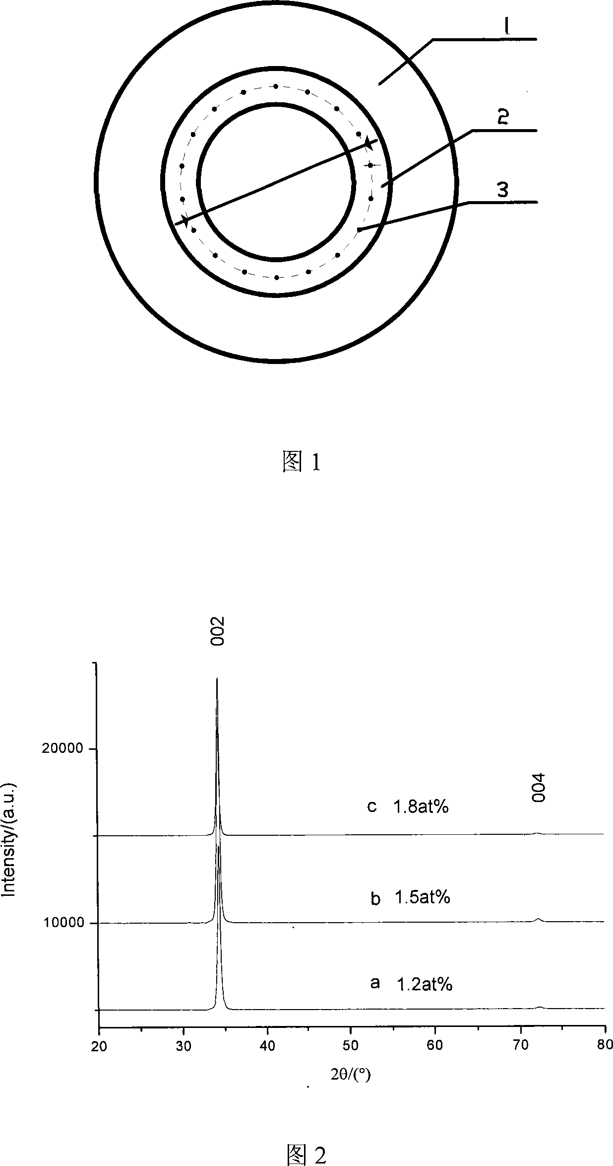
[0041] Change the percentage of molybdenum to zinc in the zinc-molybdenum metal target: 1.2% and 1.5% respectively, and the rest of the preparation conditions are the same as in Example 1. Its X-ray diffraction pattern is shown in Figure 2.
[0042] The thickness d of the film was measured with a surface profiler (Kosaka ET3000 type), and the sheet resistance R of the sample was measured with a four-probe instrument (BD-90 type) 0 The resistivity ρ of the film was thus calculated. At room temperature, the Hall effect of the thin film was measured using a Hall tester (BIO-RadMicroscience HL5500 Hall system), so as to obtain the carrier mobility and carrier concentration of the thin film. The crystal structure of the film was analyzed by X-ray diffractometer (XRD) (Rigaku D / max-rB type, CuKa ray source); the surface morphology of the film was analyzed by atomic force microscope (AFM) (Park Scientific Instrument, AutoProbe CP, USA). appearance.
PUM
| Property | Measurement | Unit |
|---|---|---|
| thickness | aaaaa | aaaaa |
| electrical resistivity | aaaaa | aaaaa |
| area | aaaaa | aaaaa |
Abstract
Description
Claims
Application Information


